This thread has been locked.

If you have a related question, please click the "Ask a related question" button in the top right corner. The newly created question will be automatically linked to this question.

TPS62130 transient response

Other Parts Discussed in Thread: TPS62130, LP38852, TPS62160

Hello,

I got similar problem when the load decreases. I used the EVM board:

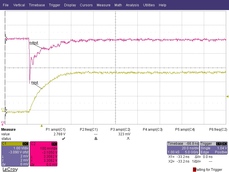
Load is 0.5A, output voltage is set to 3.3V, Vin is 12V (short wire, 10A power supply).

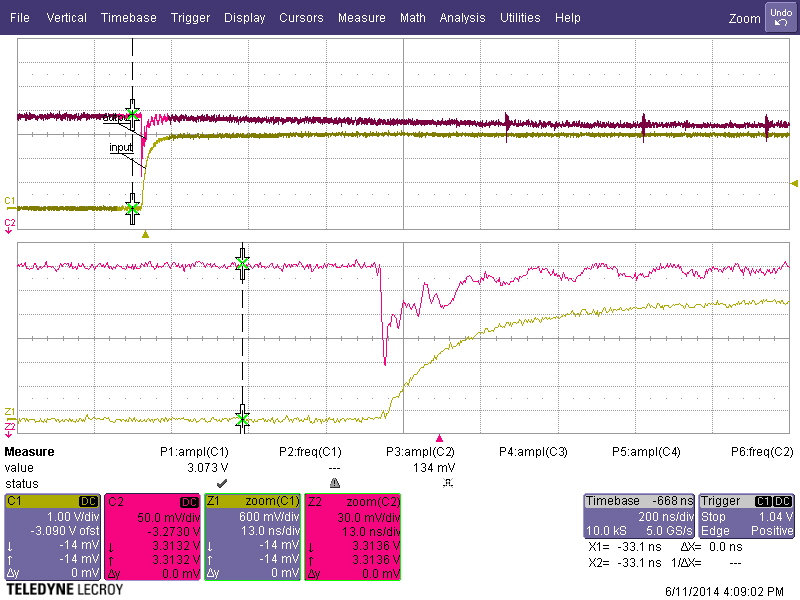
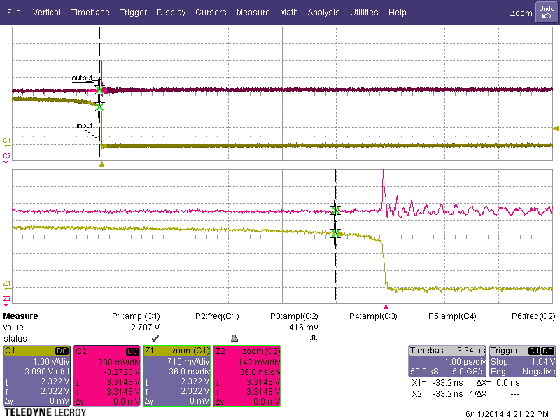
SInce I read this post, I already put a big cap of 100uF on the input and additional 100uF cap soldered on the terminals behind (cannot see in the picture above. Here is what I get: (load is 6.8 Ohms which means about 0.48A)

Please advise how to solve the problem. Increasing Cout does not help so much.

  • It is not clear what your problem is.  Could you rephrase your question?

    As well, I don't think adding a wire onto the FB pin is a good idea as this will pick up noise.

  • TI declare in the EVM datasheet that the transient reponse is 20mV when the load is connected and 20mV when the load is disconnected:

    This graph is taken from the EVM datasheet http://www.ti.com/lit/ug/slvu437a/slvu437a.pdf

    So why do I get a transient of 100mV when I disconnect a load of 480mA (which is much less than "1A to 2A" declared in this graph?

    When I bought this evaluation board I saw that graph and only because of the low transient I spent 100$ on purchasing this evaluation board (including shipping). Now I see that the load transient is 5 times bigger so I'm asking what should I do in order to get the same transient response as in the datasheet.

  • That waveform you show loos like it is due to the inductance of your wire and an instantaneous load dump.  We usually measure the load transient with a controlled slew rate.  Int he waveform from the EVM users guide it is about 400mA/usec.  In that case the transient response will be as shown.

  • Yes, the ~50 nsec wide pulse in your screenshot is not the transient response but is just noise picked up by the probe.  You need to measure the voltage change with a low inductance probe right across the output capacitor.

  • I reply to Chris and John:

    I read your comments about inductance and noise and I thought that maybe because my load was inductive, the scope probe picked up some noise which was induced by the wire wound resistors.

    Therfore, I built a new setup:

    The load is 3.5 Ohms, made from 6 SMD resistors 1206 size of 20 Ohms each.

    THis load cannot handle so many watts but for few seconds it works well. It also has no inductance.

    As for the oscilloscope and the probes: I changed the oscilloscope to LECROY model 64Xi which is a 10GS/S , 600 MHz oscilloscope. I used active probes model HPF1500 which are for 1.5GHz with 0.7pF and 100 K Ohms resistance. THere is no inductance at all. THe probes are mounted on pins soldered on the capacitor of 100uF that I added at the output (Tantalum, low ESR, 150 milliOhms) and on the load. THe channel connected to the load is the trigger channel (what is called "Input" on the pictures that would follow). The "output" is the voltage on the Tantalum cap which I added. Here is a picture of my new setup:

    Here is teh picture when the load is connected:

    Here is a picture when the load is disconnected:

    The power supply is intended to power a microcontroller with FPGA which consume current at high rise times. The suggestion of John to connect the load very slowly is actually "cheating" ourselves. I hope that you would not offer me to connect the load thru a 50Watt rheostat as some circuits were running 50 years ago...

    TI write in their web page: "optimized for applications with high power density". WIth all the respect, 400mA/usec is definetly not high power density. FOr such a slow slew rate, I can use a LM7805 regulator or equivalent.

    Among the "application" that TI suggest we see:

    Mobile PC's, Tablet, Modems, Cameras

    Solid-State Disk Drives

    Embedded Systems

    WIth all the respect, those are all applications which consume current in pulses. As you may understand, the suggestion to limit the slew rate of the load is not relevent. No one can limit the load connection time in an embedded system or a solid state drive or a laptop which works at hundreds of MHz.

    I also hope that a spike of 1 volt when a load is disconnected (about 30$ of the supply voltage) is unacceptable in any of the above examples. Most of those systems burn if you supply 4.3V olts to them. (3.3 + 1V of the spike).

    So please advice. You probably got plenty of those EVM boards there in TI so please try to simulate the problem. Thanks.

  • I don't know what happens to this editor... After I attach one picture, I cannot edit the text or add pictures any more. Here are the missing pictures:

  • Thanks for explaining your system requirements in more detail.  We have no limit on the slew rate at the output.  John was just stating the test conditions used for the UG waveform.  We cannot test every possible combination of load transient and slew rate, so we just show a few examples.  Thank you for testing an EVM to get the desired performance for your system.  This is the right way to do it.

    Your waveforms are too short a timescale to be showing the transient response.  5nsec/div and 20nsec/div is too fast for the IC to even see the change at the output and respond.  So, what you are measuring is either noise or the drop across the output cap's ESL.  You are not measuring the IC at all.  See the timescale for the waveform in the UG for an example of how much time in takes to view the waveform.

    The inductance we are concerned about is in your measurement point.  You are using a good probe and now measure across the output cap in the proper place.  Improvements to your setup might include measuring across a ceramic cap instead.  This is a lower ESL component and also allows the scope probe 's tips to be closer together--this reduces the loop area created by the probe and this reduces the noise pickup.

    What are the load transient requirements that you need to meet?  You said 12Vin, 3.3Vout.  What is the load current step from and to?

  • One more thing:

    When you see a rising edge on the green trace (which is the load resistor) it means tha tteh load was connected.

    A falling edge on the Green trace means that the load was disconnected.

  • Thanks for your quick response. FIrst, I did not change the load within 5 or 20 nSeconds as you think. I just applied one change which is just a sample of what happends during a change in the load.

    I can send you a picture with a different time base but then you won't see anything - not the rise time of the load (green trace) and not the overshoot which is created due to this load change. The sampling rate of the oscilloscope would be too slow to capture that spike.

    As you may see, TI says in thir datasheets that this chip is good for laptops. What is the speed of a Laptop? 2 GHz? 3GHz? This is exactly Nano seconds. Do you know how much current is drawn when the CPU start to write to a memory device (even if it is an external disk or other). Now imagine that there are such fast current changes which occure every few tens of nanoseconds or microseconds. How would the output voltage look like? There would be negative spikes of 300mV and positive spikes of 1 volt! I'm sorry to say but this is not what I call a "Regulator" because it does not regulate anything.

    Since I believe that TI does not write things just to satisfy their sales people, I ask you to contact the people who designed this chip and show them my graphs and ask hte same whether there is some solution for that problem.

  • The step of the load is from zero to about 900mA. 6 resistors of 20 Ohms in parallel make about 3.4 Ohms.

    Look at my setup picture. The red wire is connecting or discoonecting this load.

  • The timescale on your waveforms is 5 or 20 nsec/div.  And the rise time of the 'input' signal (which is your load current?) is around 50 nsec.  So, your rise time is very fast.  This is ok for us.

    Yes, many types of end equipment have rise and fall times this fast.  But this energy comes from the capacitors.  From I = C dV/dt, a small dt in the nsec range will not cause a significant dV on the voltage bus.  It takes some time for the output to drop, the regulator to see the drop and respond, and then for the voltage to come back.  This is a load transient test and is showed with a wider timescale as we have in the datasheet and user's guide for the EVM.

    Is your load step 0 mA to 900 mA?  I ask because you used 0.5A in your first post.  We can take some load transient responses with your specs.

  • THere are no "interesting" signals after teh time window that I captured.
    Today, digital signals are fast. A 0.8$ microprocessor works up to 20 MHz. ... We use an embedded system and we got fast signals at all frequencies up to 2.5 GHz (optical port) and a FPGA which works at 250 MHz.

    I tried different capacitors up to 200uF but it does not change the situation. I did not exceed 200uF because I read in this post teat teis is the maximum output capacitance for this chip.

    The step size was changed to 900 mA because I wanted to be "closer" to teh specs in the EVM datasheet (1A to 2A).

    However, it is teh same problem with 0.5A step. Maybe the amplitude is a little smaller.

    Please do some tests using 500-900 mA.

    Thanks!

  •  

    Following you can find the tests done on the EVM:


    1 - Load transient from 0 A to 900mA


    2- Load step from 0 A to 900 mA, added 100uF output cap:

    zoom in picture:


    Best regards

  • I see that you are using the same slow load with a very slow rise time. If you read the correspondance above, you may understand that such a load does not simulate the applications which this IC was designed for and what is declared by TI on their datasheet.

    Why won't you take a simple resistor (made from SMD resistors as I did) and simply connect it with your finger as I did. This would simulate real digital loads with high rise time and not the fancy benchtop load with round edges and very slow and smooth rise time that you connected. Did you ever saw a digital circuit which consume current with a rise time of 200nSec as in your oscilloscope drawing? Maybe 25 years ago...

  • I followed your indication to test the EVM, this is my set up:

    - 12 Vin, 3.3V Vout, 3.5ohm power resistor as load ( ~ 0.95A)

    - I use a current probe to measure the load current and a low inductive probe on the output ceramic capacitor for Vout, and switched the load manually.

    Follow the results:


    Zoom in:


    We have a SR about 800mA/500nS, and with our set up we don't experience overshoot above the 20mV as well as the EVM app note.


  • Whether the slew rate is 200 nsec or 2 nsec won't significantly affect the resulting output voltage drop.  At these speeds, the first voltage drop is from ESL.  This ESL is from the output cap, board trace, and measurement point.  ESL in ceramic capacitors is very small.  If smaller ESL is needed, low value (0.1uF, etc.) are used since they have very high self-resonant frequencies.

    As an example, consider the first waveform you posted in your post with 3 waveforms.  This is about a 300mV drop in about 2 nsec.  For the 22uF output capacitor to supply your 1A for 2 nsec would result in a voltage drop (from capacitance) of less than 1 mV.  So, this drop must come from ESL in the component or measurement setup.  

    Try adding a small ceramic at the output and measuring across this to get a cleaner measurement.  In any case, it is not the job of the power supply to respond to 2 nsec pulses on the output.  This is actually impossible considering control loop bandwidths and output inductors limiting the slew rate to the output.  This is the job of a cap.

  • To all of the support people:

    I'm sorry to say that we are going in circles. I'm trying to explain you that testing with such a small load does not simulate the problem and you tell me to use Ceramic caps and showing me again and again the same picture of your electronic load with the slow rise time. I start to wonder maybe my English is so bad and maybe I did not make myself clear enough...

    I'm sorry to say that I am very disappointed from your answers and from the fact that TI is selling a chip for high speed applications where high current loads are switched very fast and instead of trying to solve the problem you tell me again and again that I put a 5 nSec pulse where every one can see that I connect my load in a  a step, not a pulse! Is it really so unclear in my oscilloscope pictures?

    and I did try to put 5 ceramic caps of 22uF/35V one on the top of the other instead of this Tantalum cap but it does not really help. And I'm sorry to remind you again but I'm using your EVM board. Not my PCB routing. Is it so difficult to simulate the problem?

    Do you expect me to risk my entire design to have 4.3V spikes from your switcher? Do you really think that I will risk the reputation of my company and sell such a product which is deemed to be dead after a small usage period?

    Do you really think that memory devices, FPGA's or other expensive IC's can sustain 4.3V spikes on their VCC for a long time?

    I would suggest that you will offer me another regulator which can work in the same setup, with low noise and would not output 4.3V spikes.
    I think that you should also send me a free eveluation board for the new device just to compensate me a little for the 100$ I paid for the TPS EVM and all the time I was wasting in this forum.

  • I think we are talking past each other here.

    We are testing on the same board as you (the EVM) and not with an electronic load.  The first waveforms were taken with a MOSFET mounted right on the output header as the load.  This produces very fast edges.  The second waveforms were taken in the same way as you, with a discrete resistor.  Apparently, you have faster hands than we to get a little bit faster rise times.  An electronic load would be much much slower.

    A step or a pulse is the same thing to me.  My point is your rise time of the load current.  This is 20 nsec or so as shown in your waveform (the current goes from 0 to 900 mA in around 20 nsec).  How long it lasts is somewhat irrelevant.  The point is that such a fast load transient does not test the power supply but rather the capacitor.  You should be able to turn off our device, connect a lab supply to the output and perform the same test with the same timescale and test setup and get the same result.  At 20 nsec/div, no power supply can respond to this.  Only a low impedance capacitor can.

    But I am confident that the spikes you see are not real.  It looks like you are probing across the tantalum cap and taking the load current off of his exact point.  There is likely some ESL or noise pickup in your measurement.  Try probing across C3.  This is right at the output of our device and is where we have measured and see no spikes.  These high frequency measurements can be difficult.

  • I decided to give it another try and after I removed my tantalum 100uF cap, I installed a "tower" of 5 ceramic caps on the top of C3, added another 100nF low ESR cap and moved my probe and the load to C3. Here is my current setup:

    So you are right. If I probe across C3 and not across the output terminals, I get much better results. When connecting the load:

    When disconnecting the load:

    In order to avoid any comments about my "5nSec pulses", I adjusted the oscilloscope to a relatively slow sampling rate so you can see the results in a slow sampling rate on the top 2 screens and with a high sampling rate on the bottom 2 screens.

    As you may see on the top screen on the red graph, there is a high amplitude short pulse and after it there is a very long overshoot. THis ling overshoot is what we see in your oscilloscope curves. We see only this low amplitude overshoot because your oscilloscope does not sample fast enough and it does not capture the short pulse.

    PLease note that the oscilloscope has 2 time bases: THe time base on the right hand side (200nSec or 1 uSec) is for the top

    Therefore, my conclusions are:

    1, The PCB routing of the EVM board is bad. You should remove the output terminals to the bottom side of the board, below C3. You should also solder C3 on the board and make space for soldering 5 more ceramic capacitors. THe 2 output terminals should be below all of those caps.

    2. Your oscilloscope is too slow and it is missing the short impulse at the beginning. It is not a problem of a fast or slow finger... (sorry but mine cannot be replaced...)

    3. The ceramic capacitors do not solve the problem completely. They just reduce it.

    4. The TPS62130 is not well compensated for high load and cannot be compensated because it cannot allow an external capacitance of more than 200uF. I hope that all of you understand that using 10 ceramic capacitors in order to get those 200 uF and reduce the spike much more is not cost effective and it takes a lot of PCB space. This bank of capacitors cost at least $1.80, no matter if I built it from 22uF or 33uF or 47uF or 100uF caps for 6.3V or more.

    I wonder if you got any other cost effective solution?

  • Just one more note:

    On the oscilloscope plots posted now, channel 1 and channel 2 got one time base (200nSec or 1 uSec) and channel Z1 and Z2 got another time base which is noted in the square named Z1 or Z2 (13 or 36 nSec per division).

    The lightened area in the top 2 channel is shown in the zoom picture on the bottom 2 channels (Z1 and Z2)

  • Good job in getting better results by changing your measurement point and using lower ESL caps.  This should help point you in the direction that it is not the IC causing the behavior you see.  How wide would the bandwidth have to be to output a 2 nsec wide pulse?  Such a short pulse cannot even make it through the inductor, which limits the slew rate.  It simply does not make sense that you blame the IC for this behavior.  

    The response to a load transient is measured as in all of our D/S and those of other companies.  We understand that a load transient is primarily measuring the bandwidth of the control IC and the time domain response.  This is why they are shown at longer timescales.  This is the time it takes for any IC to respond to a change in operating point (such as load).

    Since your longer timescale scope plots do not show a typical load transient behavior in the output voltage (going down a little and then coming back to the regulated level--a 'v' shape), I must conclude that somehow your test method or setup is not adapted to the proper measurement technique.  To debug this, you could take some transients on the normal EVM and compare them to our D/S.  You should get very nearly the same curves.

    The TPS62130 can support a very wide output filter range--well past 200uF.  See the app note on the product page from several years ago.  Most applications do not require this at all, but many applications have this much sitting on the output bus across the board.

    Finally, I will note that this IC has been around for several years and I do believe this is the first time I have ever heard of someone asking about this topic.  (You can search this forum to check that assumption.)  I would be utterly shocked if this were actually real and a real issue in a system.  

  • I hate to tell you that, but it seems that all you care is to "protect" the good name of this IC. Please click on page #1 on this post and look at teh graph published by TI people by themselves:

    (Matteo Mencarelli1, a TI employee)

    Do you see the same spike in a red circle?

    Do you agree that this spike is in every EVM board and it does not depend on my fingers? Do you agree that this pulse is "Typical" for all TPS62130 designs?

    Since you say it is not a fault of TI, I must tell you that I use many switch mode converters for over 20 years and those phenomena do not exist in Linear and Maxim IC's that I use.

    You wish to think that this chip is marvelous design because it is sold in millions of pcs

  • ...all around the world but this is not a merit of quality or of a good design... Cigarrets are also still sold in billions of pcs and they cause death and deseases...

    I hope that you also agree that the PCB design of the EVM is bad. The + out should not come from the inductor to the right. It should be from those expensive caps and down.

    When I conside the cost/performance of this chip along with the cost of 200uF ceramic capacitors, the decision is not to buy this chip.

    Can you offer me another chip which does not have such impulses?

  • I don't think that is typical.  I've tested a lot of circuits (I've been in this a long time) for transient response.  I don't recall seeing that (but I have to admit I don't support this particular IC).

  • ...and last thing: Do you see the letters "BWL" on the oscilloscope plot published by Mr. Matteo Mencarelli1?

    (in the 2 small squares on the left bottom corner). Since I also got a LECROY oscilloscope I can tell you what it is:

    This is a 20 MHz. bandwidth limit.

    I think that it is either dishonest or just luck of knowlege to limit the bandwidth to 20 MHz. and then claim that you don't see any 5 nanosecond pulses...

    It is also unfair to sell an EVM board without C3 assembled and tehn tell only users who complain that you need to assemble 5 caps on those 2 pads if you want that circuit to work without 1V spikes...

    Please tell your colleague to open the bandwidth limit and publish his graph (with no BWL) in this post as well in the EVM datasheet. When you sell a product, you should declare the correct specifications and not hide them using oscilloscope filters or an electric load with very slow rise time...

  • Hi,

    We showed a BW limiting to show a cleaner waveform with less noise, BW limit helps eliminate the very large magnitude and short time pulses, which are noise and mainly depend on how the probe is held, what angle etc.  Noise is influencing the measurement.  Also it is clear from my plot that the probe picks up also the SW signal.  That is noise as well. 

    Follow you can find the waveforms took without BW limit:


    Zoom in:

    New waveforms without BW limit show no spike at turn on of load, the SW node in the waveforms (short time) does not move since the IC cannot respond in such short time, that’s why I can’t assume a chip fault or a contribute of the IC to generate that spike.

    You don’t need to add 5 caps on the output unless his application requires very low voltage droop during the load transient response, moreover ceramic caps are the best combination of performance and cost.

    At this link  you can download TINA simulations which show the impact of ESL, as you can see the ESL alone causes this droop. Also you can download a trial version at TINA at this link www.ti.com/tool/tina-ti

    I think we’ve discussed this topic to death and you ask for another device.  So, what power requirements does your application have?  What is your power need? Can you give us more details about the application?

  • What we need is a chip which will convert from 9-16V to : 1.2V @900 mA (with current bursts) and another one to 3.3V at 600mA (less high current bursts). THe first one (for 1.2V) is connected to a LATTICE FPGA (ECP2M35) and the other one (3.3V) is connected to a 125 MHz. A2D + 2.5 GHz. optical transmitter.

    Low noise devices are required because it is an analog circuit.

    The circuit should be relatively small. The whole PCB should go instead LP38852 (1.2V) or instead of LM7805 + TPS73701DR in hte current circuit borad (for 3.3V).

  • What are the peak current requirements?  If absolute low noise is a must, are you considering using LDOs for post regulation?

  • Assuming the current values mentioned are peak currents, the TPS62160 is a very small device to meet those needs.