This thread has been locked.

If you have a related question, please click the "Ask a related question" button in the top right corner. The newly created question will be automatically linked to this question.

TPS54295 a lot of problems

Other Parts Discussed in Thread: TPS54295

We have been trying to use TPS54295PWP in our design, and there are a lot of issues with the ICs. We have built around 15 boards and 4 to 6 boards failed with the following symptoms:

1. Output SW1 or SW2 pin shorted to ground. (Found up to 3 cases in our First Article Test Build. We have carried out detailed experiments, peak current in the system never exceeded 500mA in any case).

2. The system does not power up. (Found up to 2 cases in our First Article Test Build, the VREG5 pin measures around 5.6 V and the power supply just does not wake up).

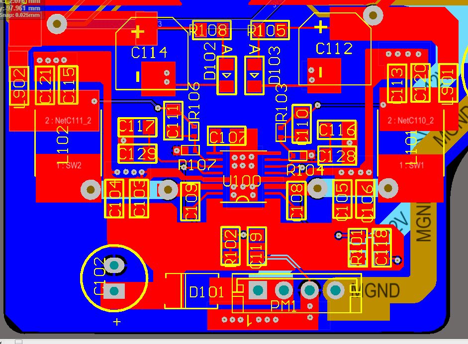
Is there any special consideration required for the design apart from the WEBENCH generated schematic and PCB Layout guide lines in the data sheet?

I have attached the Schematic accordingly. Please let me know if you need any detailed information on the failure.

We need to resolve this issue ASAP or we have to move on to select other type of Switch Mode ICs in our design.

Regards

Aung

Schematic Prints.pdf
  • I can see some issues with your design.  For the input voltage rails, you need a minimum of 10uF x5r or x7r ceramic capacitance directly coupled to the VIN1 and PGND1 and VIN2 and PGND2 pins.  That is 2 total, one for each side.  C110 and C111 are too big.  I would start by just removing them or using 10pF for each.  Your slow start time is very long.  I would reduce C128 and C116 to 10nF total.  Same for C117 and C129.  The extra filtering on the output may be interfering with the converter.  Try removing L901 and L902.  Se if both output start up properly.  Let me know your progress.  

  • Thanks Jhon,

    Is your suggestion for the startup issue only?

    How about the issue that Output SW1 or SW2 pin shorted to ground?

    Regards

    Aung

  • For the input voltage rails, you need a minimum of 10uF x5r or x7r ceramic capacitance directly coupled to the VIN1 and PGND1 and VIN2 and PGND2 pins.  That is 2 total, one for each side. 

    Is it the reason that the IC sometimes does not wake up properly? May I know the effect of putting smaller capacitors at VIN1 and VIN2?

    C110 and C111 are too big.  I would start by just removing them or using 10pF for each

    Could this be the reason that  Output SW1 or SW2 pin shorted to ground? 

     Your slow start time is very long.  I would reduce C128 and C116 to 10nF total. Same for C117 and C129. 

    I was trying to make sure the IC Startup properly with output capacitors C112 and C114 (100uF), which was not recommended in the design. The reason that we have tried to have a long slow start time was an attempt to solve the problem of the SW1 or SW2 pin shorted to ground, we needed the 100uF IC on 3.3V and 5V output rails as reservoirs for the MCU PIC32MX460F512L-80I/PT (3.3V) and USB (5V), and we had a hypothesis that start up in rush current into 100uF reservoir 100uF capacitors might be a cause of the failure  Output SW1 or SW2 pin shorted to ground. 

    Please help to explain a little bit more on this.

     Try removing L901 and L902. 

    The reason that we have put L901 and L902 was to protect too much in rush current going into 100uF capacitors at the output ( C112 and C114 ). Are you sure removing them won't damage the SW1 or SW2 due to too much in rush current at start up into them?

    Regards

    Aung

  • I have attached the layout as well for your reference.

    Thank you.

    Aung

  • Here is the new finding for problem number 1.

    There is a strange symptom in one of our PCBAs, 

    - The temperature of the area near the IC, around 80 degrees

    - The 5V output goes haywire, it goes between 6.5 V and 5 V intermittently.

    The failure mode which could cause 5V rails to go higher than the specified voltage is really bad news for us (6V in this case but we might expect to see higher voltages in certain situations, as I could see some ICs in 5V rails failed with the Switch mode IC failure).

    Please suggest the root cause to this problem as well.

    Regards

  • The layout for dc/dc converters in general is critical.  You have to keep the circulating current loops short and use wide low impedance traces.  This is especially true for the input bypass capacitors.  All the switching ac current go thru them and it is critical to keep the parasitic inductance low.  High voltage spikes are the usual cause of internal FET failure.

    I suggested that you remove L901 and L902 completely to isolate the TPS54295 circuit from the external load and additional capacitors.  I think you would be best to get the circuit up and running reliably first, then troubleshoot the down stream problems.

  • Thanks John,

    I have exactly follow the layout guide lines, i don't think we have layout issues.

    After reading the application note on D-CAP2TM http://www.ti.com/lit/an/slva546/slva546.pdf, I understand more on this.

    As the topology of the IC is based on hysteresis control (not error amplifier), with so called "ripple injection" additional circuity to improve the frequency response (it simply adds a zero to the system) making the system more stable.
    Any output LC variant could shift the pole further from the zero (picture below), so I am thinking of removing the 100uF output caps forever.
    And putting 100nF in the circuit makes the system unstable because this IC only have a comparator inside (not error amplifier), and we are supposed to add caps in pF to improve the phase margin compensating the effect of the delay factor. (Hd(s)), it simply adds pole-zero pair to the system.
    In conclusion, I will to do the following:
    1. Remove the 100uF output caps
    2. change the 100nF caps accross the feedback resistor to smaller values (10pF is recommended by the TI Tech: Support)

    Regards

    Aung