This thread has been locked.

If you have a related question, please click the "Ask a related question" button in the top right corner. The newly created question will be automatically linked to this question.

Current Limiting problem in TPS54360

Other Parts Discussed in Thread: TPS54360

Hi,

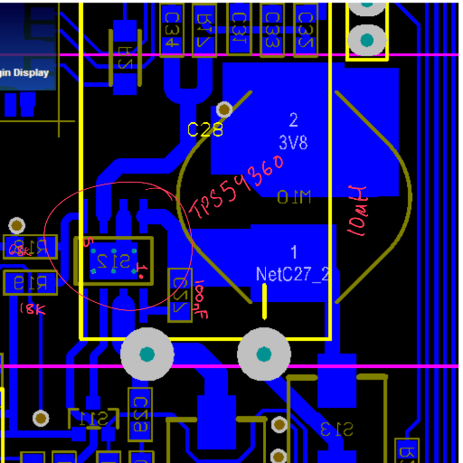
I have designed a power supply for GPRS modem using TPS54360. My Input voltage range is from 8V to 60V and max current is 3A and output voltage is 3.8V

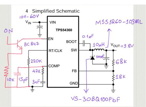
Sorry the values of the RC components with the compensation (COMP) are wrong in the above circuit. I have used R=12k (instead of 47k) and 10nF (in series with this resistor, instead of 3nF) and then 15pF (parallel to the R and C). I have used the formulas in the datasheet to calculate these values. I have gone through the datasheet a couple of times and reconfirmed all the values and everything seems correct.

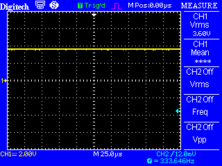
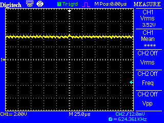
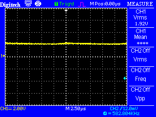
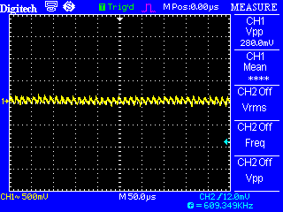
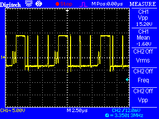
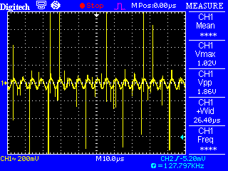
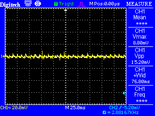
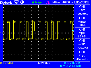
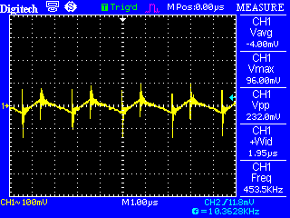
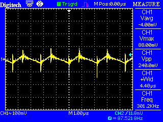
Everything works fine till 900mA and as soon as I put on some more load the output voltage drops to 1.8 or ~2V (depending on the load) and as a result of voltage drop current also drops.

Can anyone please tell me what am I doing wrong? Thanks in advance.

Regards

Saqib

  • Hi,

    I am waiting for the reply....

    Thanks guys.

    Regards

    Saqib

  • Can you post some waveforms?  Be sure to include the switching node.  Please show the normal operation and then just after you raise the current.

  • If this was tested on a custom board I would also like a screenshot of the layout. Noisy layout is known to contribute to performance like you described.

  • Hi,

    Thanks for the reply.

    Below are the waveforms;

       <-- No Load Waveform

      <-- At ~800mA load

      <-- When I tried to increase the load to ~1.6A, the voltage drops to 1.92V and as a result of which current goes to ~750mA 

    I have also noticed that output ripple is too much. 

      <-- Output ripple

    I was using a 100uF/16V capacitor first and was getting a 500mV ripple. Then I increased the capacitance to ~700uF but still 280mV ripple is huge (@800mA load)

     <-- SW output....I don't think it should be like this, I might be doing something wrong but don't know what....

    It might be the layout problem. The layout is given below;

    I have disabled the Top layer so that you can see the regulator. All the remaining area of the board is grounded.

    Waiting for the feedback. Thanks.

    Regards

    Saqib

  • Hi,

    Can someone please reply back....Thanks.

    Regards

    Saqib

  • The circuit looks unstable, but I bet it is a layout issue.  I do not see any ceramic input capacitor tied tightly to VIN and GND. It looks like you only have an electrolytic.  It should be ceramic X5R or better.  The RT resistor should be located very close to the IC and terminated directly to GND  The rectifying diode placement is not optimal as well.  I do not see your output capacitors or their return to GND either.  Closely compare your layout to the recommendations on page 36 of the datasheet.

  • Hi John,

    Thanks for the reply. I will check it out and will get back to you.


    Regards

    Saqib

  • Hi,

    I have made the circuit on a separate board and soldered all the components right on the IC pins. 

    At the Vin I have 470uF/50V (elco), 4.7uF/25V (tantalum) and a 100nF (ceramic) ----> Vin = 12V

    And at Vout I have 100uF/35V (elco), 10uF/25V (tantalum) and 100nF (ceramic) ---> Vout = 3.8V

    I have tested the circuit till 2A and this time output voltage is not dropping. But the ripple on the output voltage is still too much. Please have a look on the following waveforms and tell me what might be going wrong. 

     ---> Vout (AC coupled at 0.6A) and at 2A load Vpp reaches to 4.2V

     ---> Vout (AC coupled under No load)

     ---> SW (at 0.6A)

    Please reply back as soon as possible. Thanks.

    Regards

    Saqib

  • It looks like you still have stability issues.  The SW waveform should be a steady pulse stream, not short and long pulses.  Also you should consider at least 10 uF X5R or better ceramic capacitor directly across the VIN to GND.  The large voltage spikes re switching noise.  They may be an artifact of your measurement.  You have to measure VOUT ripple directly across your output cap.  Use a very short (< 1cm ) ground lead.  "tip and ring" technique is best.

  • The stability issues are most likely caused by the layout. The ceramic capacitor recommended by John can also help.

    The placement of the ceramic input capacitor and schottky diode are very important. The ceramic input capacitor should be located as close as possible to the VIN pin with as low of an inductance trace possible. The diode sould be located as close as possible to the SW pin with as low of an inductance trace possible. The ground of the input capacitor and diode should be as close as possible with as low of an inductance trace possible, this connection is typically made on the large ground plane. Please see the EVM layout for an example. When there is a large amount of inductance in either of these paths it adds a lot of switching noise that can interfere with the internal control circuits.

    To reduce the effect of the inductance you could try a different diode. What diode are you using? An RC snubber across the diode can also reduce the switching noise. However I recommend also improving the layout.

  • Hi,

    Thanks for your replies.

    I am using 30BQ100PbF, its a 100V, 3A Schottky diode.

    Anyway I will remake the circuit and keep the recommendations in mind and get back to you in a day or two.

    Thanks.

  • Sounds good. The 100V diode could be contributing to the issues. You may see some improvement with a 60V diode like the MBRS360.

  • Hi,

    I have made another circuit and tried to make it as close to the recommended layout as possible. It's not on a final PCB, it's on a SO-8 breakout board. I only had 10uF/6.3V ceramic so have only used 470uF/50V (elco) and 100nF (ceramic) on the input side and a 100uF/25V (elco) and 100nF (ceramic) at the output side. The results are much better as compared to previous circuit.

      --> SW at 600mA load

      --> SW at 2A load

      --> AC coupled Vout at 600mA load

      --> AC coupled Vout at 1A load

      --> AC coupled Vout at 2A load

    It's better than previous circuit but there is still a significant high frequency noise. I will try with some better capacitors and also with a 60V catch diode. Do you think that it's still the layout issue or some capacitance issue?

    Thanks.

    Regards

    Saqib