This thread has been locked.

If you have a related question, please click the "Ask a related question" button in the top right corner. The newly created question will be automatically linked to this question.

LM5050-1 Gate working Principle

Other Parts Discussed in Thread: LM5050-1

Hi,

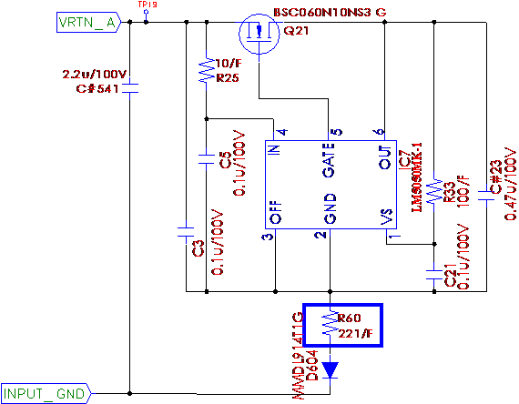
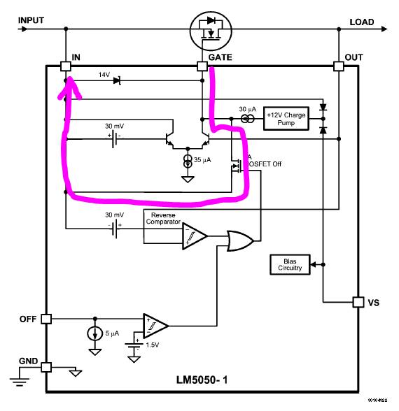
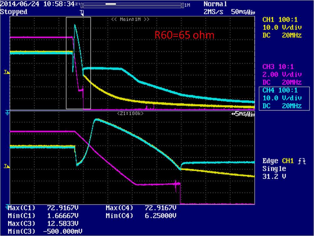
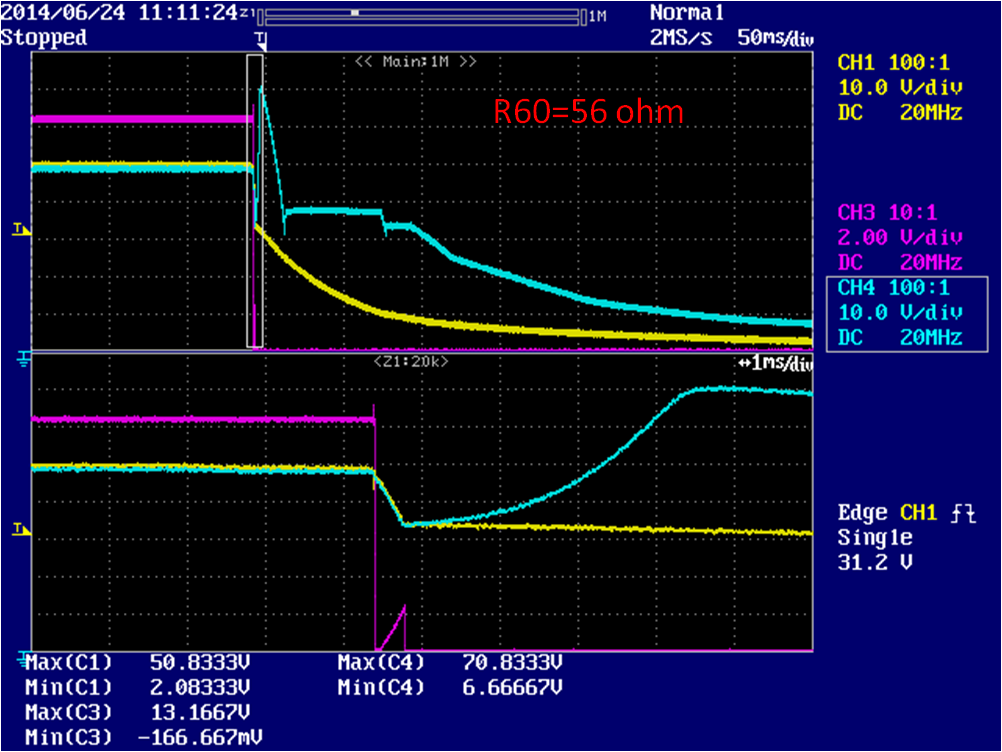
One of our cusotmer used below cirucuit for LM5050-1 and found the R60 will effect the turn off speed of Q21 when input shut down.  Q21 will turn off quickly with a small R60 when input shuts down.

Can you help to check and give an explain for this phenomenon? if we should kill R60 in a real applicaiton?

Thanks.

Oliver Ou

  • Hi Oliver,

    The diode is used for reverse input voltage protection. I don't typically see a resistor in series with it. Please see page 14 of the datasheet Figure 31 as an example.

    Regards,

    Darwin

  • Hi TI‘s member,

    could you please explain the principle of gate charge and discharge.From block diagram,the gate discharge path hace no relationship with R60.But we found the gate discharge slew rate affected by R60.

    if possible,please give me the e-mail(lu.yun@deltaww.com.cn) .

    Johnny

  • Johnny,

    The 2A gate current sink is not characterized under that particular design condition. Having a resistor in series with the diode at the GND pin is not recommended and not what we have see in the past. We recommend this be removed.

  • Hi Darwin,

    I don’t know the real reason although the testing indicate the R60 has impact on gate’s discharge slew rate.

    Is it right that gate discharge path showed on the picture in last . Please correct me if I’m wrong.

    Anyway, I need the exact gate charge and discharge path, thanks!

    Johnny

  • Hi Johnny,

    The discharge path that you have drawn is correct. Do you know why this resistor was placed there? 

    Do you have a waveform we can look at that compares the resistor and without resistor (0 ohm) showing VIN, VS, GATE, VOUT?

    We believe that the VS pin, that powers the part, may be effecting the fault ciruitry and drive of the GATE pin during a fault. You can try removing the resistor on VS and powering it with a separte/clean power supply or increasing the VS cap to verify this. 

  • Hi Darwin,

    please refer to below waveform:R60 used 65ohm and 56ohm。

    you can see when i use 56 ohm the gate waveform(pink color) drop sharp.

    i want know the root cause.

    if you want to any picture please contact me(lu.yun@deltaww.com.cn).

    thank you!

    johnny

  • Hi Johnny,

    What are the other traces showing? Were you able to test the VS pin with a separate supply? Also, I saw you have a resistor in series with IN pin. This is not shown in the datasheet. In order to narrow down the issue. the system needs to be in a typical configuation as shown in the datasheet. Then you can see what change to the design is causing this when the resistor in the GND pin is added.

  • Hi Darwin,

    yellow color is show input voltage,

    blue color is show output voltage.

    but i don't know why the R60 can effect the gate normal operation.

    How about IC internal working?

    johnny

  • Johnny,

    We have looked into the internal design of the IC and it is not different from the block diagram. This is why we are interested in external design such as the VS.

    We believe that the VS pin, that powers the part, may be effecting the fault ciruitry and drive of the GATE pin during a fault. You can try removing the resistor on VS and powering it with a separte/clean power supply rather than at the output.