This thread has been locked.

If you have a related question, please click the "Ask a related question" button in the top right corner. The newly created question will be automatically linked to this question.

TPS53355EVM vias effect

Guru 20090 points
Other Parts Discussed in Thread: TPS53355

Hello,

Please see the attached image.
TPS53355 has the many vias around the input/output capacitor and Vin/GND line.
Could you please le me know these vias effective ?

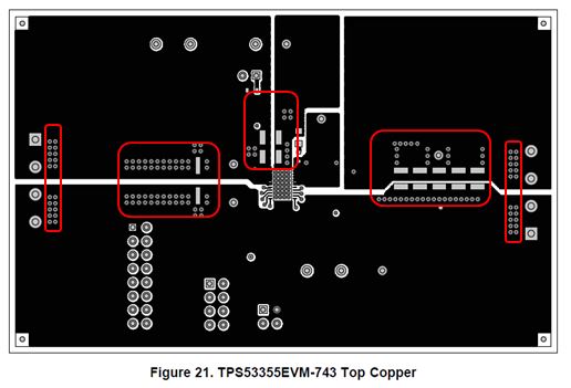
In my customer boards has large EMI noise.
Then they are confirming this for the possibility of reduce the EMI.

Best Regards,
Ryuji Asaka

  • The EVM is 6 layers.  The vias tightly couple the top side ground area to the internal and bottom side ground copper areas.  Additionally, on the bottom layer are extra VOUT and VIN copper areas.  There are additional vias to connect the top and bottom VIN and VOUT areas.  Layout is a big factor for EMI.  Reducing the circulating current paths and minimizing the parasitic inductance can help a lot.

  • Hello,

    Thank you for the reply.
    I understand that the reason as the following.

    -ensuring the high current paths
    -reducing the circulating current paths
    -minimizing the parastic inductance

    Best Regads,
    Ryuji Asaka