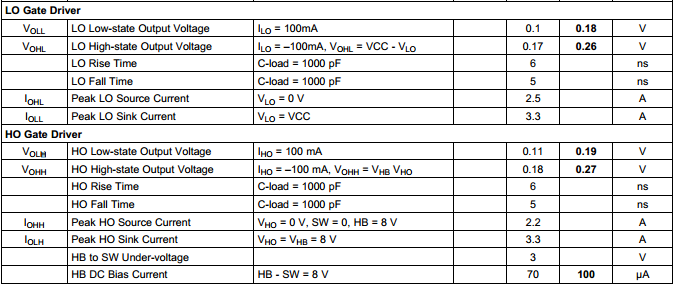
I am trying to find the min, typ, & max levels for the Low side MOSFET gate drive pins (LO1&2) & the High side MOSFET gate drive output pins (HO1&2). Is this equal to the VCC level minus some drop?

-
Ask a related question
What is a related question?A related question is a question created from another question. When the related question is created, it will be automatically linked to the original question.