This thread has been locked.

If you have a related question, please click the "Ask a related question" button in the top right corner. The newly created question will be automatically linked to this question.

D-CAP explained

Other Parts Discussed in Thread: TPS53126, TPS51218, TPS51727, TPS51220, TPS40131, TPS40100, TPS40180, TPS40130, TPS40140, TPS54327, TPS51461, TPS51125, TPS51216, TPS51463

Hello,


My customer is looking for an explanation of the D-CAP principle.

I checked and found the document  SLVA281b.

There seem to be three flavours being D-CAP, D-CAP+ and D-CAP2

Can someone explain the differences between the three?


Another question is why TI uses many voltage control DCDC's in stead of current mode control.

Is there an advantage of one over the other?

  • This app note explains the tradeoffs between current and voltage mode control

    http://focus.ti.com/general/docs/litabsmultiplefilelist.tsp?literatureNumber=slua119

    I don't know of an app note explaining the differences between the flavors of D-CAP mode.  But by reading the descriptions from different datasheets, we can note some differences.  Always refer to each device's datasheet for an explanation of how that particular device is designed and meant to be used.

    From the TPS53126 (D-CAP2): does not require ripple on the output for regulation

    "The main control loop of the TPS53126 is an adaptive on-time pulse width modulation (PWM) controller that supports a proprietary D-CAP2 mode control. D-CAP2 Mode control combines constant on-time control with an internal compensation circuit for pseudo-fixed frequency and low external component count configuration with both low ESR and ceramic output capacitors. It is stable even with virtually no ripple at the output. At the beginning of each cycle, the high-side MOSFET is turned on. This MOSFET is turned off after internal one shot timer expires. This one shot timer is set by the converter input voltage ,VIN, and the output voltage ,VO, to maintain a pseudo-fixed frequency over the input voltage range, hence it is called adaptive on-time control. The one-shot timer is reset and the high-side MOSFET is turned on again when the feedback voltage falls below the reference voltage. An internal ramp is added to the reference voltage to simulate output ripple, eliminating the need for ESR induced output ripple from D-CAP mode control."

    From the TPS51218 (D-CAP): requires output ripple to regulate

    "The D-CAP™ mode uses the ESR of the output capacitor(s) to sense current information. An advantage of this control scheme is that it does not require an external phase compensation network, helping the designer with ease-of-use and realizing low external component count configuration.

    "

    From the TPS51727 (D-CAP+): output voltage set by VID

    "The TPS51727 is a DCAP+™ mode adaptive on-time converter. The output voltage is set using the 5-bit VID code defined in Table 3. "VID-on-the-fly" transitions are supported with the slew rate controlled by a single resistor on the ISLEW pin."

    Note that you posted to the external forum.

  • Chris,


    Thanks for the answer.

    DO you know of any TPS devices with external FETs that operate in current mode control rather than voltage mode control?

  • Most every external FET boost controller is current mode.  But just go to the power parametric search and click on controllers: http://focus.ti.com/paramsearch/docs/parametricsearch.tsp?family=analog&familyId=433&uiTemplateId=NODE_STRY_PGE_T 

    Then, filter by current mode PWM.  We get the TPS51220, TPS40131, etc.  Note that multiphase controllers are usually current mode as this helps with current sharing between the phases.

  • The following controllers (External MOSFETs) use Current Mode Control

    TPS40100 (Single with programmable current feedback gain)

    TPS40180 (Stackable Single)

    TPS40130/131/132 (2-phase Controllers w/ single control loop)

    TPS40140 (Sackable Dual / 2-phase

  • Hello Chris

    My custmer ask us to probe gain/phase for a DCAP2 device "TPS54327". I reject his request because DCAP2 don't need to probe it. His end customer ask us to explain it. I would like tell him as "The main control loop of the TPS54327 is an adaptive on-time pulse width modulation (PWM) controller that supports a proprietary D-CAP2 mode control. D-CAP2 Mode control combines constant on-time control with an internal compensation circuit for pseudo-fixed frequency and low external component count configuration with both low ESR and ceramic output capacitors." The OP in TPS54327 play as a compairtor. The OP in Voltage mode, current mode PWR IC play as a  integration & differentiation operaton. Voltage mode , current mode PWR IC need to probe gain/phase. And DCAP mode PWR IC don't need.

    Would you please give me some advice?
     

  • Actually, you can make gain loop response measurements with DCA2.  Since DCAP2 uses adaptive on time and pseudo-fixed frequency, the switching waveform is is relatively uniform.  TPS54327 is not exactly DCAP2 as there is no eternal VO pin, but you can measure the loop in the usual manner by injecting into the feedback loop.  You do need to be careful about interpreting the results however.  The TPS54327 will show a high crossover frequency and depending on the output voltage, may hve less than 45 degrees of phase margin.  It is inherently stable, as the phase is increasing at crossover rather than decreasing, so there is no danger of oscillation.

  • Hello John

    I just discuss with our customer RD and explain what's D-CAP , D-CAP+ and D-CAP2. One question. How to explain stability of D-CAP2.  Cusotmer see our formula (1)

    f0=1/(2pi * ESR * Co) <fsw/3. They think RD will need verify output cap ESR. End customer will ask they probe ESR. That's will make they trouble. Did we have simply document and explanation to "explain stable of D-CAP"?

  • That equation you reference is applicable to DCAP, not DCAP2.  DCAP 2 uses internal ripple injection to allow use of low ESR output capacitors.  for DCAP2, the loop gain at low frequencies is constant and phase is 180 degrees.  At the LC corner frequency, the gain starts to fall at -40 dB / dec, and phase drops rapidly from 180 degrees towards 0 degrees (since the output capacitor is low ESR ceramic type, the Q is high). There is an internal zero caused by the ripple injection circuit.  Phase will start to increase one decade below the internal zero frequency towards 90 degrees.  At the internal zero frequency phase will be 45 degrees and the gain slope will be - 20 dB / dec.  For DCAP2 the goal is to align the LC corner frequency near enough to the fixed, internal zero frequency, so that some conditions are met: phase does not drop to zero, final closed loop crossover is not to high, and phase at crossover is close to 45 degrees.  For DCAP 2, this means that for many applications measured phase margin will be less than 45 degrees.  You have to remember that "phase margin" is exactly that, it is margin, or a figure of how far away you are from instability, so the absolute value of phase margin is not so important, just the relative slope of the phase curve near crossover.  For ordinary voltage mode or current mode control, phase is usually dropping off rapidly at crossover, so phase margin is important.  For DCAP2, phase is actually INCREASING at crossover, so the circuit is inherently stable.  There is no chance of phase dropping to zero (oscillating) if the external L and C are properly chosen.  If additional phase margin is desired, you can add a FF cap across the upper resistor of the voltage setpoint divider.  This is mostly applicable to higher output voltages above 1.8 V.  I do have some powerpoint I did for another customer.  Contact me offline if you would like to see it.

  • Dear John

    May I have you powerpoint about DCAP2 stablity? You may Email to my Email Box kami_haung@yosungroup.com as my myTI acccount.

  • Dear All,

    for the D-CAP+ control loop, is it available an application tool, in order to calculate the right value for Rc and Cc?

    In my application are using the TPS51461.

    Many thanks,

    Rosario


  • Hi Rosario,

    Please contact Rama Venkatraman directly. He is the system engineer for TPS51461 and should have the design tool for Rc, Cc calculation. His email address:

    rama-venkat@ti.com

    Thanks,

    Nancy

  • John. I cannot find in the literature at what frequency the zero is introduced for the DCAP2. 

    Leonard.

  • It is proprietary and not published.  If you measure the loop you can infer the approximate location based on the deflection points.

  • H, FYI.

    Please refer to the below puiblished application note regarding a frequency response model about DCAP2.

    http://www.ti.com/lit/an/slva546/slva546.pdf

    Best Regards,

       K.Yoshio


  • Hi Rosario,

    I gave you a wrong contact person before. You can contact Yoshikawa Miura (y-miura2@ti.com) directly. He is in charge of this part.

    Thanks,

    Nancy

  • Hello Ti engineers

    TPS51125 TPS51216 and TPS51463 are used for PC. TPS51125 and TPS51216  are D-cap mode! TPS51216   has no FB pin and Vin pin! TPS51216  compare  output Voltage  with external REF ,Dose this  function add ripple for stability?How dose TPS51216 sense input voltage?I guess   TPS51216 gets TPS51216  input voltage information  from Sw pin!If it is ture, TPS51216 gets input voltage informatio after high mos   turn on.So Dose TPS51216 immediate adjust Ton when input voltage changes?b

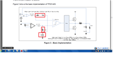
    TPS51463 is D-cap+ mode! But it is not used for Vcore! I dont find sense current pin like CSN CSP! How dose TPS51463 sense current information?I know   D-cap+
    IC campare Vdroop  with  current  feedback signal!  I find TPS51463 is differernt! Can you explain  Block Diagram belw?

    thanks for your help!


  • For TPS51216, the VDDQSNS pin is equivalent to FB pin.  There is no ripple injection built in to DCAP, it relies on ripple voltage due tho ESR of output capacitors.  Yes the TPS51216 uses the SW node voltage to sense VIN.

    TPS51463 senses current by measuring low side FET drain source voltage during the "off" time.  it is proportional to the current.

  • Hi John,

    Your explaination about DCAP2 stability is really helpful. But as you said "There is no chance of phase dropping to zero (oscillating) if the external L and C are properly chosen.". I wonder whether DCAP has limitation on the design of LC filter.

    Besides, the zero frequency is determined by output capacitor or ripple injection circuit (RC) in DCAP mode, so how to make the zero frequency suitable for loop stability?  

    Thank you ve much.

    Best regards!

    Brian Zhao