


Hi,
By means of the Webench Design Tool I made a 3.3V switching regulator design (1212.webench_design_3.3V_1.2A_general.pdf). Furthermore I made a second design (1200.webench_design_5V_1.5A_general.pdf) for 5V. Both of them are implemented at one PCB, here are the schematics: 4621.EPS_v1.5.pdf.
Now both designs have been manufactured and they show some identical problems. The supply power comes from a isolated 12V DC/DC and is fine. After putting the UVLO/EN input to 3.3V (directly connected to a µC GPIO), the SS/TRACK voltage ramps up, but collapses very quickly down to 3.2mV. The PGOOD pin has a voltage of 0.2V. According to the datasheet the switching regulator is in a fault state and swtiched of nearly everything.
It seems that the temperature is measured incorrect. The voltage at the OTP is 2.5V which is way too high (if it exceeds 1.15V, an overtemperature fault is detected and the switching regulator switches of everything). So I measured the voltage at the D+ pin to see what is measured by means of the NPN transistor. Here is a picture:
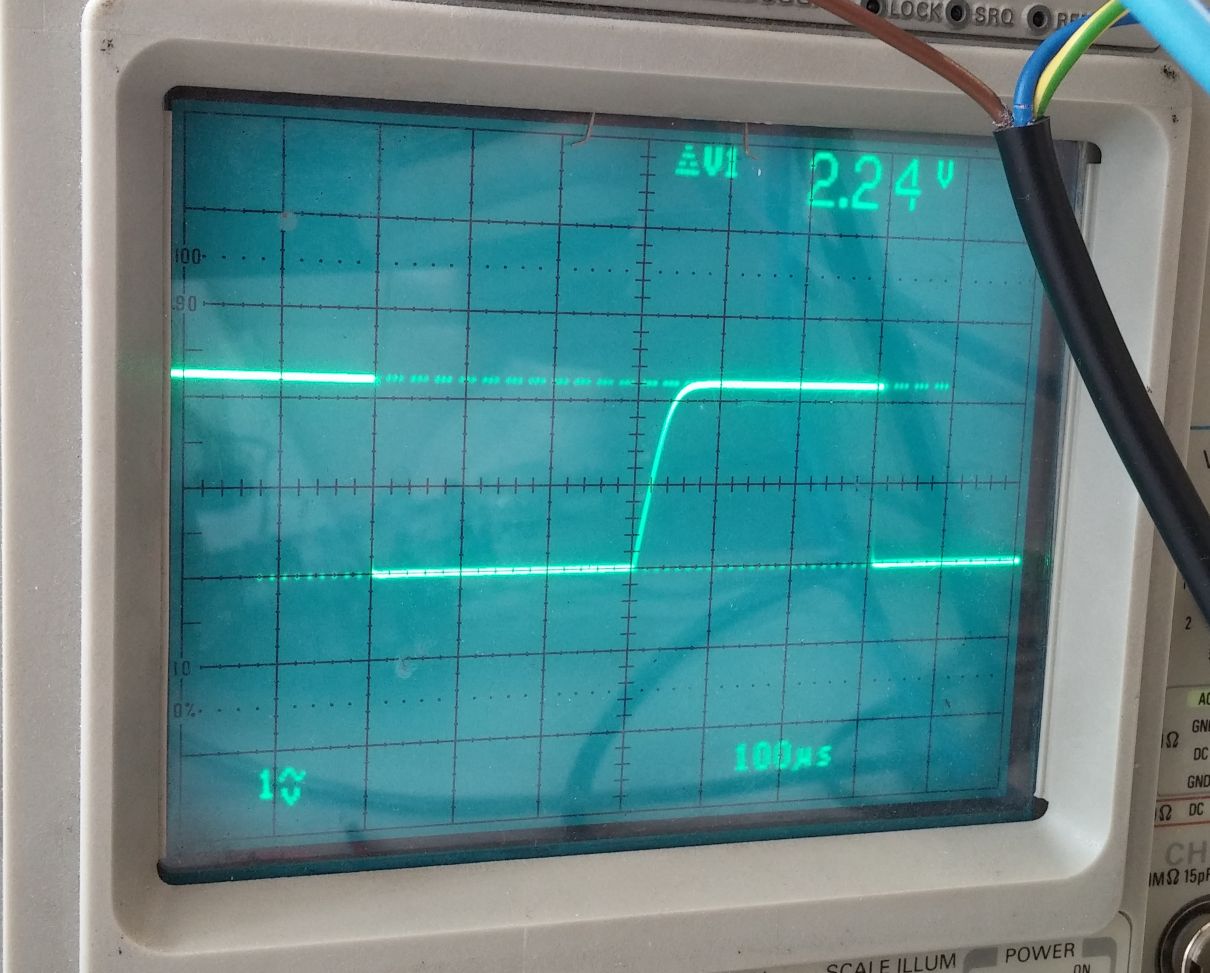
Here I can see a deltaVbe of 2.24V which is also way too high. The PCB is at room temperature.
Now I am out of ideas, somehow the temperature seems to be measured incorrect, but I don't have any idea why.
To ensure that the overtemperature is the reason for not starting, I connected the OTP pin to GND (which disables the overtemperature feature). Furthermore I connected the FADJ pin to GND as well to increase to the maximum switching freuency. In this case, the switching regulator starts correctly and is working as expected. But only in this case.
Doas anyone has an idea what could be the problem?
Thanks a lot in advance!


