This thread has been locked.

If you have a related question, please click the "Ask a related question" button in the top right corner. The newly created question will be automatically linked to this question.

LM5010MH output drop across input range

Other Parts Discussed in Thread: LM5010

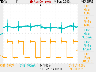
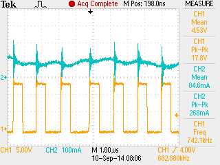
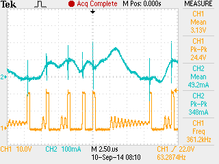
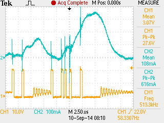
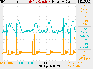
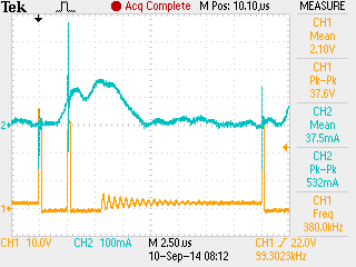
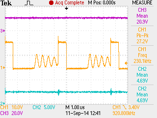
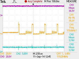
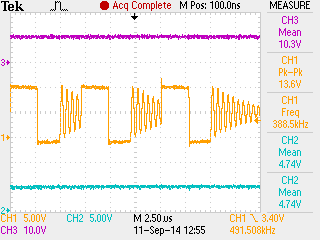
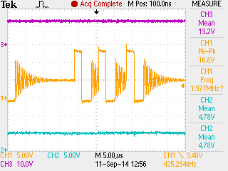
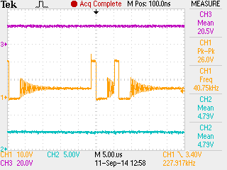
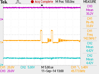
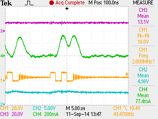
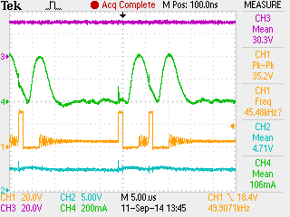
Hi, I'm trying to use the LM5010MH to convert input voltages in the 10V to 48V range down to 5V.


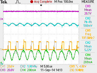
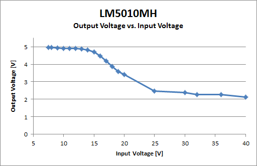
The design works fine for low voltages but the output drops to an unusable level above 15V.  Here is a graph with more data points:

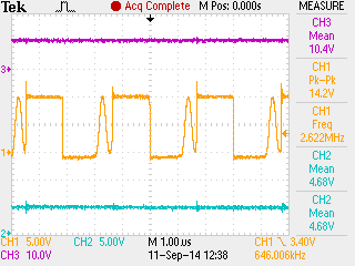
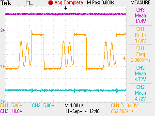
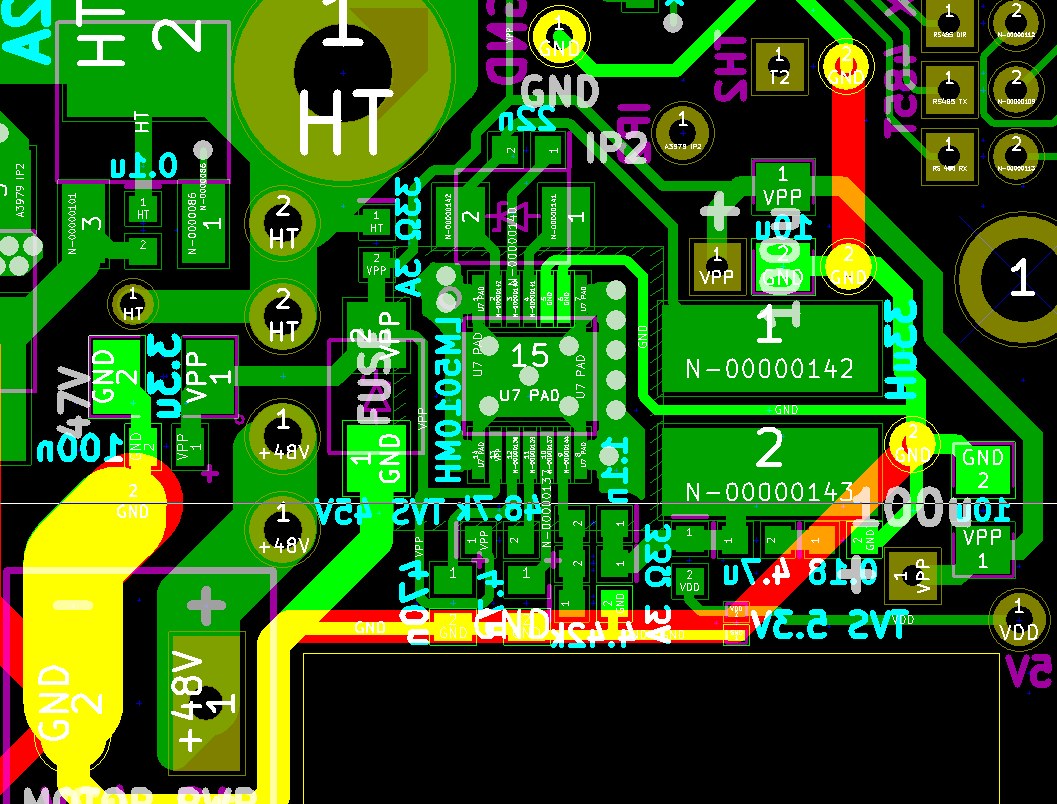
Here is the schematic for my circuit:


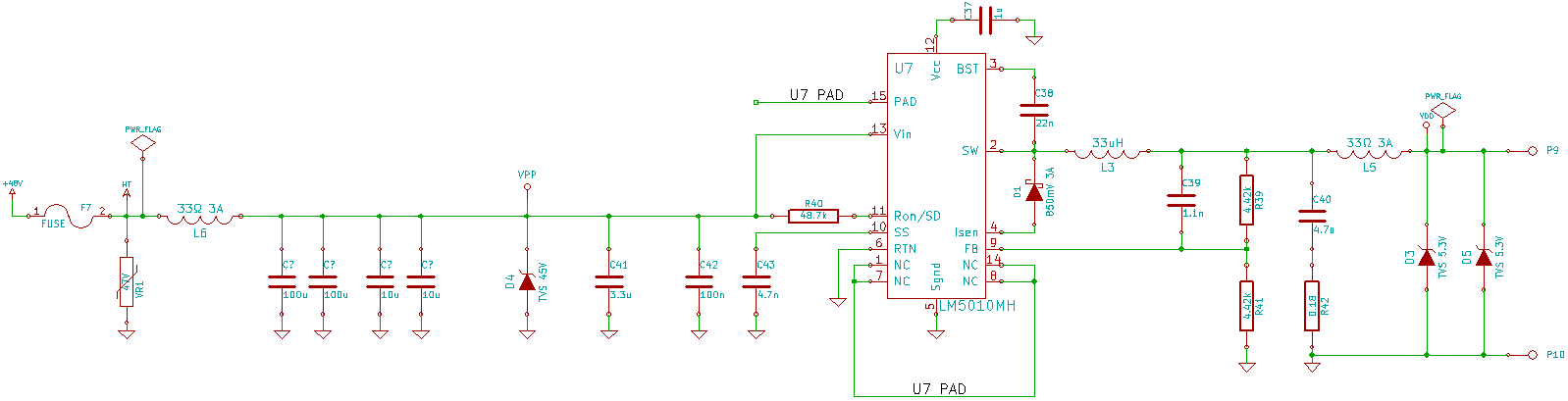
The inductor symbols labeled "33ohm 3A" are SMT ferrite beads. 

I've also attached the Webench design that the implementation above was based on.  I tried to use the exact parts listed in the Webench bill of material.

I would like to increase the range of input voltages to the LM5010 that will give me 5V on the LM5010 output.  Any thoughts or ideas for troubleshooting?


Thanks!


- Chris

7563.LM5010 Webench Report.pdf

  • Hi Chris,

    Can you share the inductor current waveform and SW node waveform when the part works and when it does not?Regards,

    Vijay

  • Hi Vijay, thanks for the reply!

    In the scope traces below CH1 is the SW node voltage and CH2 is the inductor current.

    This is for an LM5010 input voltage of 10V, which gave an output voltage of 4.84V (the part is working correctly):

    This is Vin = 13, Vout = 4.63V (the part is working correctly):

    These next two are both Vin = 20V, Vout = 3.026V (the part is not working):

    These next two are both Vin = 30V, Vout = 2.120V (the part is not working):

    Obviously some differences in the outputs.  What do you think this suggests?


    Thanks!

     - Chris

  • What is the load current? Also inductor current does not look like usually inductor current waveform. How are you measuring it?

  • I'll have to measure the load current tomorrow.  For what it's worth, as I recall (I could be wrong), the input current starts off around 50mA and drops down with the voltage. 

    To get the current waveform I used a Fluke 80i-110s AC/DC current clamp connected to my Tektronix o'scope.  To take the measurement I de-soldered the inductor and used two wires as risers to lift the inductor off of the PCB pads.  Then, I put the clamp around one of the wires.  Is there something else you would recommend?  A current sense resistor or something else?

  • The way you are measuring the current seems ok. But your inductor current waveforms don't look right. They should be triangles. Also the webench design suggests ~500kHz switching frequency. The waveforms are ~750kHz.


  • The inductor ripple current is predicted in the webench design to be 100's of mA. But the pictures show much smaller values.

    Is there a gain term on your current scope.

    I good way to start debugging the circuit will be to reduce the frequency using the RON resistor (say to 100k(ohm) or 200k(ohm)).

  • I actually just saw that the current clamp specs say the usable frequency is DC to 100 kHz...

  • The clamp does have two settings: one for 10mA/V and another for 100mA/V. 

    I confirmed that the readings were correct by first measuring the current through a resistor with a known voltage and resistance: the clamp did give report a value very close to the theoretical value. 

    However, I think the operating frequency might be too high for the clamp since it only goes to 100 kHz according to the specs.

    I will play with Ron tomorrow.  If you can think of anything else to try, let me know and I'll report back my findings.

    Thanks for your help!

  • Load current tests:

    Vin [V] Iin [A] Vout [V] Iout [A]
    10 0.04 4.82 0.078
    13 0.03 4.50 0.074
    20 0.02 4.19 to 4.75 0.066 to 0.075
    30 0.02 3.13 0.051

    At Vin = 20, it looked like it was on the boarder of working / not-working.  The waves looked mostly good but it would glitch every once in a while with the decaying sine waves as in the previous post.


    The output current was measured with a Fluke 789 meter as well as the clamp connected to the o'scope.  The means were in close agreement.  The trace did have some noise in it: the peak-to-peak went between 40 to 80 mA.

    I'll try increasing Ron now...

  • Yes. Nothing stands out other than relatively high fsw. Useful to see <500khz result.

  • Here are the results from changing Ron from 48.7kΩ

    CH3 is the input voltage, CH1 is SW node voltage, CH2 is the output voltage

    Ron = 100kΩ, Vin = 10.4V, input current = 0.04A, load current = 81mA:

    Ron = 100kΩ, Vin = 13.4V, input current = 0.03A, load current = 81mA:

    Ron = 100kΩ, Vin = 20.9V, input current = 0.02A, load current = 81mA:

    Ron = 100kΩ, Vin = 30.3V, input current = 0.04A, load current = 63mA:

    Ron = 200kΩ, Vin = 10.3V, input current = 0.04A, load current = 83mA:

    Ron = 200kΩ, Vin = 13.2V, input current = 0.04A, load current = 83mA:

    Ron = 200kΩ, Vin = 20.5V, input current = 0.02A, load current = 82mA:

    Ron = 200kΩ, Vin = 30.2V, input current = 0.04A to 0.1A, load current = 72mA to 76mA:

    Changing Ron to 200kΩ made the maximum usable input voltage go up to about 23.5V, which is an improvement but still a long way from the webench design of 50V.  I'll try increasing Ron more: do you think increasing Ron/decreasing the frequency could cause any negative issues?

    Thanks!
    - Chris

  • What do you mean by "fsw"?

  • Hi Chris,

    You have specified in the webench design 1A load. Does the regulation change for different VIN at hgiher loads.

  • After changing Ron to 200kΩ I can now see the triangles in the inductor current waveform (CH4) you were expecting:

  • Vin [V] Iin[A] Vout[V] Iout[A] Vout(pk-pk)[mV]
    10 0.13 4.75 0.24 380
    13 0.10 5.09 0.24 440
    20 0.07 5.22 0.242 520 to 600
    30 0.04 3.36 to 4.7 0.200 to 0.204 720 to 960

    Here's the o'scope for 20V, these all have Ron at 200kΩ:

    Vin [V] Iin[A] Vout[V] Iout[A] Vout(pk-pk)[mV]
    10 0.16 5.04 0.280 360
    13 0.12 5.06 0.280 440
    20 0.07 4.72 0.260 640
    30 0.04 3.57 to 4.01 0.204 760 to 1040

    When doing our design, we didn't know the exact current output we would need.  The above is close to worst case: we probably will never have to supply 330mA.

  • Is it possible to increase the output capcitor. If you can please try increasing it to 15uF or 22uF for this test.

    Also the increase in the output voltage with VIN makes sense (first table)

    decrease in output voltage with VIN does not make sense (2nd table).

    I may at some point need to look at the layout of your board.

  • I tried webench again with a 0.33A output current specification and it suggested using a 100uH inductor.

    With 101uH for the inductor value and Ron = 200kΩ I got:

    Vin[V] Iin[A] Vout[V] Iout[A]
    10 0.04 4.81 0.080
    20 0.02 4.24 0.072
    30 0.07 2.65

    0.046

    But the maximum working input voltage went down to 17.4V.  I define this as the maximum voltage where the LCD doesn't flicker.

    CH1 is SW, CH2 is Vout, CH3 is Vin, CH4 is inductor current. 

  • Actually I was going to ask this before, but have you tested with a resistive load?

  • I will try to change the capacitor tomorrow.

    My whole problem is that the output voltage decreases when the input voltage increases.  It was the reason behind by original post.  There is a tipping point: the output voltage does increase with increasing Vin up to a point, but then at the tipping point the output voltage starts to decrease with increasing input voltage.

    Here's the layout of the dc-dc portion of the layout:

    The LM5010 is in the middle on the bottom layer.  The top layer over the LM5010 is copper filled to dissipate the heat, but it's not shown here as it would just make everything harder to see.  You can see the vias though that connect to the top copper filled pad.

    Thanks again for your help!

  • A purely resistive load?  No, I have the DC-DC converter integrated into my circuit.  I have only tested it in the circuit where I need it to work for my application.

  • Progress!

    With Cout = 10uF, L = 33uH, Ron = 200kΩ:

    Vin Iin Vout
    26 0.01 5.02
    28 0.01 4.79
    30 0.01 4.12

    With Cout = 20uF, L = 33uH, Ron = 200kΩ:

    Vin Iin Vout
    26 0.01 5
    28 0.01 4.8
    30 0.01 4.16

    With Cout = 24.7uF, L = 33uH, and Ron = 200kΩ:

    Vin Iin Vout
    26 0.01 5
    28 0.01 4.78
    30 0.01 4.14

    So the maximum working Vin moved up a few volts.

    With Cout = 24.7uF, L = 33uH, and Ron = 100kΩ:

    Vin Iin Vout Iout Vout pk-pk
    30 0.01 4.1 0.062 0.76

    So not an improvement over Ron = 200kΩ

    With Cout = 34.7uF, L = 33uH, Ron = 200kΩ:

    Vin Iin Vout Iout Vout pk-pk
    26 0.01 5.02 0.077 0.32
    28 0.01 4.84 0.074 0.36
    30 0.01 4.24 0.065 0.4

    So a minor improvement over Cout = 24.7uF

    I'll keep playing.  Let me know if you have suggestions for tweaks.  Thanks for your support!

  • Hmm, I noticed that the results are better if I have an o'scope probe connected to the SW pin.

    The only difference between this trial and the above is that in the below results I had an o'scope probe on the SW pin.

    With Cout = 24.7uF, L = 33uH, and Ron = 200kΩ:

    Vin Iin Vout Iout Vout pk-pk
    8 0.05 5.07 0.076 0.24
    10 0.04 5.08 0.078 0.28
    12 0.03 5.09 0.079 0.32
    14 0.03 5.09 0.078 0.32
    16 0.02 5.09 0.078 0.32
    18 0.02 5.09 0.078 0.36
    20 0.02 5.09 0.078 0.32
    22 0.02 5.09 0.079 0.36
    24 0.02 5.08 0.078 0.4
    26 0.02 5.09 0.078 0.4
    28 0.01 5.07 0.076 0.56
    30 0.01 4.99 0.075 0.6
    32 0.01 4.59 0.07 0.52
    34 0.01 4.28 0.065 0.52
    36 0.01 4.11 0.063 0.56
    38 0 4.04 0.061 0.56
    40 0 4.07 0.061 0.52
    42 0 4.08 0.062 0.52
    44 0 4.13 0.062 0.56
    46 0 4.23 0.064 0.6
    48 0 4.34 0.065 0.68
    50 0 4.45 0.068 0.72

    I replaced the o'scope probe with a 10MΩ resistor and the results matched what is in the table above.