This thread has been locked.

If you have a related question, please click the "Ask a related question" button in the top right corner. The newly created question will be automatically linked to this question.

TPS3600D33

Hi,

I want to use the TPS3600D33 in a design with 3V3 system voltage.
The memory interface works with 1V8. The battery is 3V6 and I have
to use a linear regulator to bring it to 1V8.

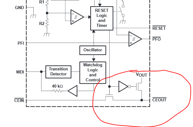
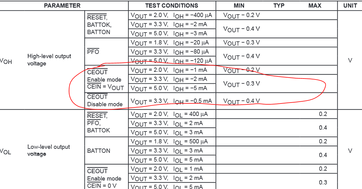
The main reason for the TPS3600D33 is the chip-enable gating.

My question: Do I need a level converter 1V8 to 3V3 for CE.in and
a level converter 3V3 to 1V8 for CE.out or is there an easier way?

Kindly regards,
Willi

  • Willi,

    The TPS3600D33's Chip Enable is a series pass-through transistor, so no level shifter should be needed. I would just expect a voltage drop across the device, and the output is referenced to Vout when the supervisor is in disable mode.

    The drop across the device will vary depending on the output load, and you would have to check the electrical characteristics table to ensure that it will still read a logic high (1.8V into CE looks like it should come out at round 1.5V out worst case into a high-Z node).

    Regards,

    David

  • David,

    thank you for fast answering. If I understand it right, I have nothing to do on input but if /CEIN is high, the level of  /CEOUT is for instance VOUT = 3.3V - 0.3V = 3.0V in standard mode and VOUT = 3.6V - 0.3V = 3.3V in battery mode.
    This would damage the CE-Input of the SRAM with VDD = 1.8V.

    My plan: The 1.8V regulator for SRAM power get VOUT as input power. Only then it is possible to use BATTOK.

    Regards,
    Willi

  • Willi,


    You are correct on your understanding. You will need a level shifter after the output of /CEOUT to shift it down to 1.8V from 3V.

    Regards,

    David