This thread has been locked.

If you have a related question, please click the "Ask a related question" button in the top right corner. The newly created question will be automatically linked to this question.

LM25575 Schottky diode failure on +12Vdc -> -12Vdc conversion

Other Parts Discussed in Thread: LM25575, LM5575

> Hello,

I have made a board using different LM25575 to manage the power supplies from a PLC backplane providing 24Vdc as shown herebelow:

- A first stage converts 24Vdc to 5Vdc,

- A second stage generates +12Vdc from the 24Vdc,

- A third stage converts the +12Vdc (from second stage) to -12Vdc.

During the power-up of the board, both +5Vdc and +12Vdc voltages are OK.

However, the Schottky diode (D3 on the schematic) of the 3rd stage has burned. We have replaced the diode with a 1N5818 but the output voltage is around +400mV.

Moreover, the diode voltage seems to be compliant with expected results (MOS open et diode close => inductor discharge) as shown on the plot below (note a 1/10 voltage probe is used) :

The frequency is also good, around 550kHz as expected with 9.09kOhm resistor on RT.

So, do you have an idea concerning the Schottky diode burning and the no -12V potential ?

Thanks in advance,

Best regards.

Alexandre

  • Hello,

    In the buck boost topology, the SW node experiences higher voltage stress. The total voltage at the SW node would be Vin+Vout. Therefore the diode needs to be rated above this threshold. You haven't mentioned what load you are pulling out of the -12V. But the current stress is also higher. At 12Vin to -12Vout, the duty cycle is rougly 50%. Therefore, the average current through the diode could be Iout/(1-D), which is 2*Iout. Is your diode rated for the right current? Also we wouldn't recommend through hole components for a high frequency SMPS.

    The C178 helps bypass noise from input to the output (the new reference for the IC). In my past experience increasing this cap up to 4.7uF has helped. Would you share some more information? We'd like to see more scope shots of the inductor current and voltage at BST pin. Also, please share your layout. PDF images would be helpful.

    Regards,
    Akshay

  • Hello,

    Thank you for your quick feedback.

    Concerning the board, I join you a document with PCBA views (power supplies and consumers) :

    2437.PCBA_mother board.pdf

    In parallel, I have order new diode reference (1N5819) and a 4.7uF 50Vcc X7R capacitor to replace C178.

    Moreover, I have take the scope shots for Vin and BST voltages as shown herebelow:

    VIN:

    BST voltage:

    zoom on start-up phase:

    Unfortunately, I can't take the current though the inductor L3.

    Is the behaviour coherent?

    Regards,

    Alexandre 

  • Re,

    I have mistake to join you a plot of the -12V potential:

    All scopes have been performed with a differential voltage probe with a gain of 1/10.

    Regards,

    Alexandre

  • Hello,

    The plots don't look normal. I am not sure why your +12V which is your input to obtain -12V is rising so slowly. The softstart cap of 10nF shouldn't be doing anything. The internal default SS time is 4.5ms. So +12V should be established within 5ms. Are you sure the 12V output is working fine? Your BOM selection does not look particularly wrong. What is your desired load current at the -12V output? I ran a webench design assuming that your load is 500mA. Please see attached design report. 3364.neg12Vo_LM25575.pdf

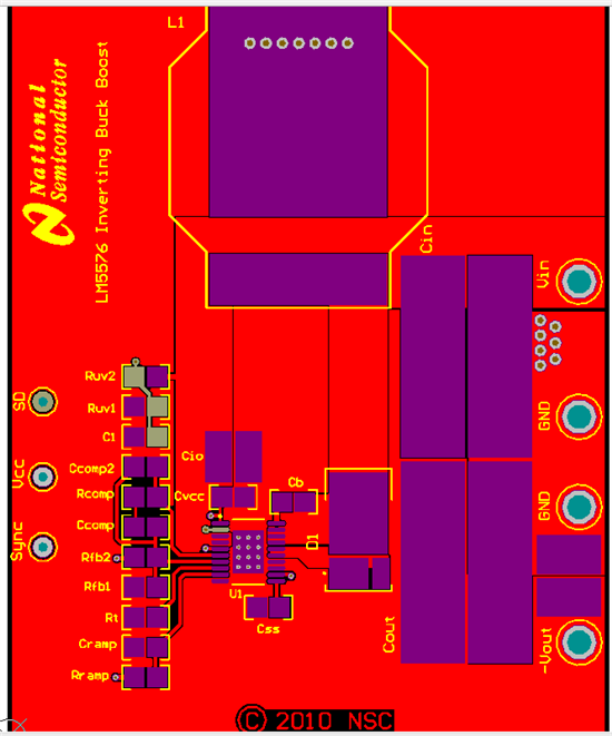
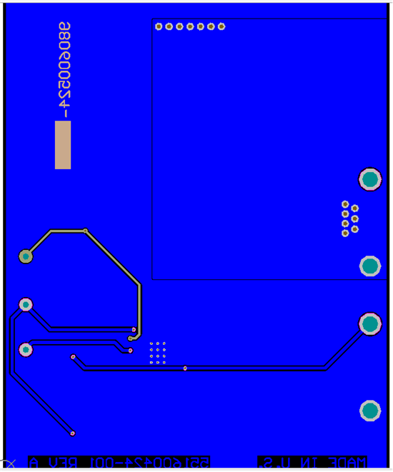
    After looking at your layout, I think you need to optimize it further. I have attached top and bottom layer pictures of our in house board. 

    The board is of the LM5575 so the pin out will be slightly different. The general idea is to avoid noisy traces and have tighter current loops. In your layout, you have used thermal reliefs which will add parasitic inductance in paths. You also have placed vias in path of sensitive nodes such as Isense and FB. single vias add more parasitic inductance. 

    Regards,
    Akshay

  • Hello,

    I have solve the problem. We had a short ciruit between the -12V potential and the ground. Indeed, the thermal pad of all converters were grounded ... We have eliminated the connection of the -12V converter to ground and now all is OK.

    Thank you for your support and help.

    Alexandre