This thread has been locked.

If you have a related question, please click the "Ask a related question" button in the top right corner. The newly created question will be automatically linked to this question.

Turn off problem with synchronous buck converter

Other Parts Discussed in Thread: UCC27201

Hello everybody.

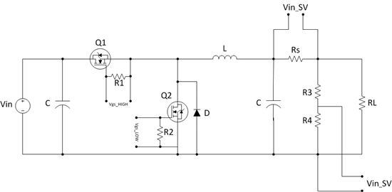
I am making a synchronous buck converter of 200kHz. It’s in open loop right now. A schematic diagram is presented in Fig. 2 and description of circuit elements are detailed on table 1.

Fig. 2. Synchronous buck converter.

Table 1. Elementos del circuito de la figura 2.

Elemento

Referencia

D

STTH8ST06

Q1, Q2

STFI40N60M2

Driver

UCC27201D

Cin

10uF/50V

R1, R2

10KΩ-1/2W

L

74435584700 WurthElectronics

C

330uF/100V

Rs

0,05Ω/5W


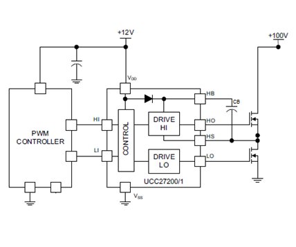
Figure 3 is a half bridge drive to switch Q1 and Q2 MOSFETs. UCC27201 is a 8 pin SOIC package of TI. The implemented circuit has a boostrap capacitor (CB) of 470nF and every MOSFET has a 6.8 Ω resistor in series with gate pins.


Fig. 3. Half bridge driver.

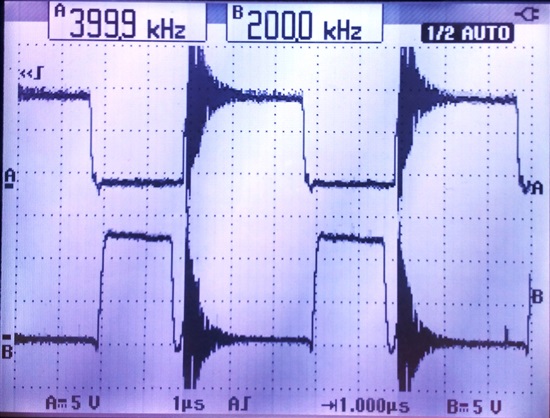
Fig. 4.  PWM Q1 signal measured from microcontroller pins.

Fig. 5. PWM Q2 signal measured from microcontroller pins.

Figure 4 and figure 5 are PWM signals for Q1 and Q2 MOFETs, respectively, measured from microcontroller pins without power stage (inductor, capacitor and low). PWM signal has a dead time of 250ns (about 5% of dutycycle).

Fig. 6. Vgs of Q2 measured from MOSFET without power stage.


Fig. 7. Vgs of Q2 measured from MOSFET with power stage.


Fig. 8. Top: Vgs Q1, Bottom: Vgs Q2, measured from MOSFETs pins with 30V powered converter and a load of 1.14 A

Converter has a 17.2V with a dutycycle of 56% but according to figure 6, PWM signals have high frequency oscillations and when Q1 is turning off and Q2 is turning on, there is a short time when both MOSFETs are ON at the same time (I couldn’t solve this problem even put a dead time of 1us which is about 20% of switching period).

Given that increase the timeout is not enough, How to improve the driving state transition from Q1 to Q2?


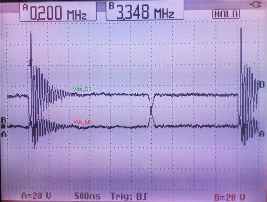
Fig. 7. Drain-source voltage.


  • Jhoan,

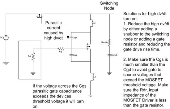
    Your wave forms appear to me to be caused by high dv/dt false turn-on, or what is often referred to as "gate step" or "parasitic" turn-on. When the top switch turns on. it puts a high dv/dt voltage on the switching node; i.e., the node where the source of the top switch is connected to the bottom switch. See the figure below. This high dV/dt causes a current to flow through the parasitic gate to drain capacitance, Cgd, and gate to source capacitance, Cgs, of the bottom switch. The two capacitors form a voltage divider. If the ratio of the Cgs to Cgd is high enough a voltage appears at the bottom switches gate that is higher than the threshold voltage and the switch turns on and causes a shoot through condition.

    The parasitic capacitances are nonlinear, so it is easier to check the MOSFET's data sheet and look at the gate to source charge, or Qgs, and gate to drain charge, Qgd. Compare them and make sure that the ratio between the Qgs/Qgd is less than one. There are other issues to consider as well. You may need to add a snubber at the switching node to reduce the dv/dt. If designed properly, the snubber circuit can actually increase the converter's efficiency by delaying the off voltage rise time and causing a zero voltage turn on condition. Power is lost in the snubber resistor so most of the time the power loss is wash. Except that with a snubber you can avoid high dv/dt parasitic turn on.

    The current, C dv/dt created by the high dv/dt at the switching node splits between the Cgs and the intrinsic gate resistor Rgi, If Cgs is small, more current flow through Rgi than Cgs. This reduces the gate to source voltage caused by Cgs, but if the input impedance of the MOSFET driver is much larger than Rgi, the voltage at the MOSFET gate can also exceed the threshold voltage of the MOSFET and cause a false turn on.


  • Chuck, thank you very much for your reply. I'll check your suggestions and then I will be reporting what happens.