This thread has been locked.

If you have a related question, please click the "Ask a related question" button in the top right corner. The newly created question will be automatically linked to this question.

CSD75205W1015 - Connecting the 2 P-Mosfets

Other Parts Discussed in Thread: BQ25505

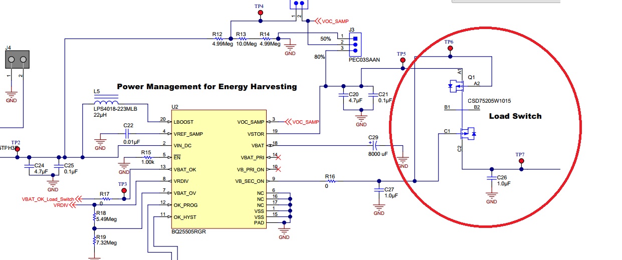
I came through this pdf in which CSD75205W1015 is used to control load power. It can be noted that there are 2 P type Mosfets in this IC.

http://www.ti.com/lit/ug/tidu235a/tidu235a.pdf on page 27 

I realised in that the two P MOSFETS are connected serially. My understanding is that it is a waste of energy. But I want to know why it has been done that way. May I know what the reason is? 


  • anyone who knows why this design practice is done?

  • The back to back FETs isolate the batteries from each other.  If only one FET, its body diode would allow current flow from one battery to the other. 


  • Thank you Jeff for your reply.


    I'm still not able to spot  two power sources (batteries) that require to be isolated in this diagram.

    The top most Mosfet is powered by the pin 19 of BQ25505RGR and both Mosfets are turned ON by VB_SEC_ON pin . I believe when the top Mosfet is ON, current flows through the bottom Mosfet towards the J5 if there is a load.
     

    But where is the second battery that need to be isolated?

    I still don’t have a clear idea as to why two mosfets have been used. I would appreciate your elaborative explanation  so much.

  • The bq25505 was designed so that it can be used to switch the load between a primary non-rechargeable battery (connected to VBAT_PRI) and a secondary rechargeable battery (connected to VBAT_SEC).  In that application you need back to back FETs to isolate the two batteries or the body diode with allow current flow from one to the other.  In our application, I now see that you are only needing a load switch to isolate the load from VSTOR so you do need back to back PFETs, only one PFET with source connected to VSTOR.