


Hello Ti,
I have some questions regarding TPS62140, and I would appreciate if someone can take a brief look and comment on schematic and rough layout.
I have performed some basic tests on EVKIT for TPS62140.
Information regarding solution.
VSYS is 4.6 - 7.5V input voltage.
Output is 3.8V
Nominal load current on 3V8 is 50mA, with transients up to 2A. The 3.8V output voltage cannot under any circumstances drop below 3.3V
C200 is placeholder for feed forward capacitor.
R204 is placeholder for setting DEF pin high.
Schematic
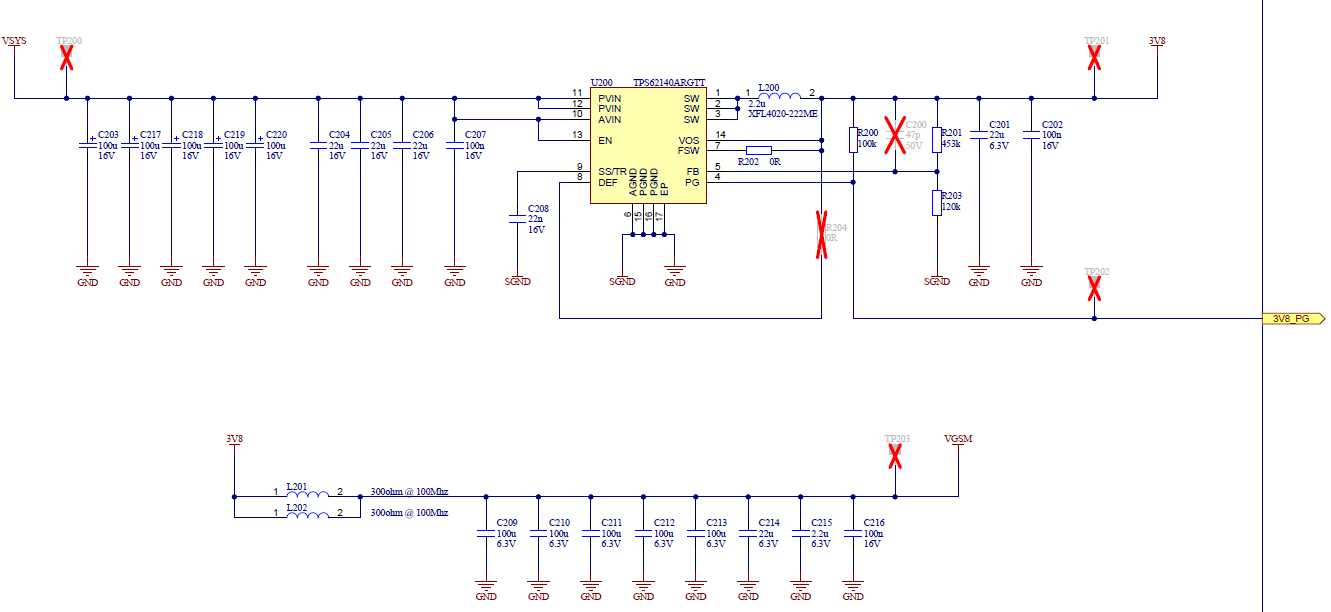
Schematic questions and sanity checks.
- How much will capacitors C209-C16, bulk capacitors for VGSM, affect the control loop of U200? Do I need to recalculate and choose new components for LC combination, new inductor etc based on application report SLVA463?
- To sustain a solid output on 3.8V during fast 2A transients, the best solution is to add mode Cout?
- DEF (pin 8) and FSW (pin 7) can be left floating when resistors are not mounted? Can i tie to output 3V8 for high level?
Layout
Bare in mind that this is just a rough layout to visual current paths and feedback loops.
Common ground on layer 2, this is a 4-layer board.
Point of load at the end of yellow path with vias down to bottom layer.
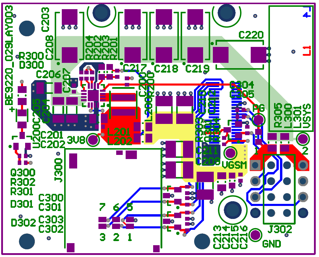
Layout questions
- Are input capacitors positioned okay?
- Bulk output capacitors positioned along path for load where space is available, positioning okay? Also related to schematic question regarding control loop stability.
- Are there any layout related improvements that you can see?
I appreciate all feedback I can get.
Best regards,
Sebastian

