This thread has been locked.

If you have a related question, please click the "Ask a related question" button in the top right corner. The newly created question will be automatically linked to this question.

TPS43060 Boost Circuit (SW node blows on power up)

Other Parts Discussed in Thread: TPS43060

Dear Specialist,

We have designed in a TPS43060 boost circuit into a new product nearing release to production to work with the following:

Vin:24V

Vout:52V

Iout: 1A

fsw: 1Mhz

The problem we are experiencing is that on power up the SW node is blowing, a spark/smoke can be seen on pin 12 (SW) each and every time.

As suggested by the datasheet we have placed an RC snubber accross the high-side mosfet and also controlled the gate of low side mosfet and boot schottky diode by placing series 4.7R resistors. By doing so we can get the circuit to work although only when we reduce Vout to 42V. 

When working with the board at 42V we noticed the SW node had significant ringing on it and the signal was not clean with over and undershooting. 

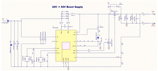
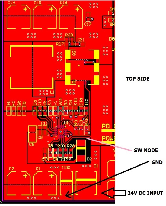
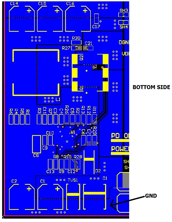
Please see top and bottom layout including schematic design below, any suggestions would be greatly appreciated as this design is in the production stage.

PCB is manufactured on 2 Layers with 2oz copper on top and bottom.

Kind Regards,

Daniel Haddad

  • Sorry I notice the schematic is a bit hard to read, following standard components as suggested by Ti's Web Bench tool have been designed in as below:

    L1            22UH/6.7A    Coilcraft MSS1210-223MED

    Q1, Q2     BSZ520N15NS3 G

    D2           MBRS1100T3G

    C12         100NF/50V    (Boot/SW Cap)

    R2           56K (RT resisitor)   

    Anything else I can provide please let me know :)

  • Hello Daniel,

    Have you had any answer to your issue? I ask because I am facing the same problem, in a circuit similar to yours. My output voltage is 54V instead of 52V. 

    Best wishes,

    Newton

  • Hi Daniel,

    Very sorry for such the long delay on this. I'm not sure how it slipped through.

    It might be too late now but I took a look over the layout and in this case I believe it was very likely layout related. The critical switching loop does not have the best bypass capacitor placement. There should be a ceramic capacitor placed as close as possible to the drain of the HS MOSFET and the source the LS MOSFET. This path is quite long.

    Additionally the connections for the AGND and PGND are not ideal. It is very likely the switching noise is getting into the analog control circuits. The layout could be significantly improved if the TPS43060 was rotated 180 degrees. The pins for driving the power MOSFETs are located closer to them and the components for the analog control circuits would be located further from the switching noise.

    Newton, I suggest checking your layout to see if you could also make improvements in regards to this.

    Best Regards,
    Anthony

  • Hi Anthony,

    Thanks for you help. We solved this problem last November and it was mainly due to the mosfets selected which was causing undershoot on the SW pin and hence the IC was blowing on power up.

    Newton, you could see how we got there on my other forum post;

    e2e.ti.com/.../380788

    Long story short if mosfet gate charge is similiar to the mosfet we used then you will need to drive the gate with a small resistor to slow down the gate charge slightly.

    You also need to be careful that your low side and high side switching ON times do not cross.

    Hope this helps, thanks guys.

    Kind regards,

    Daniel Haddad.