


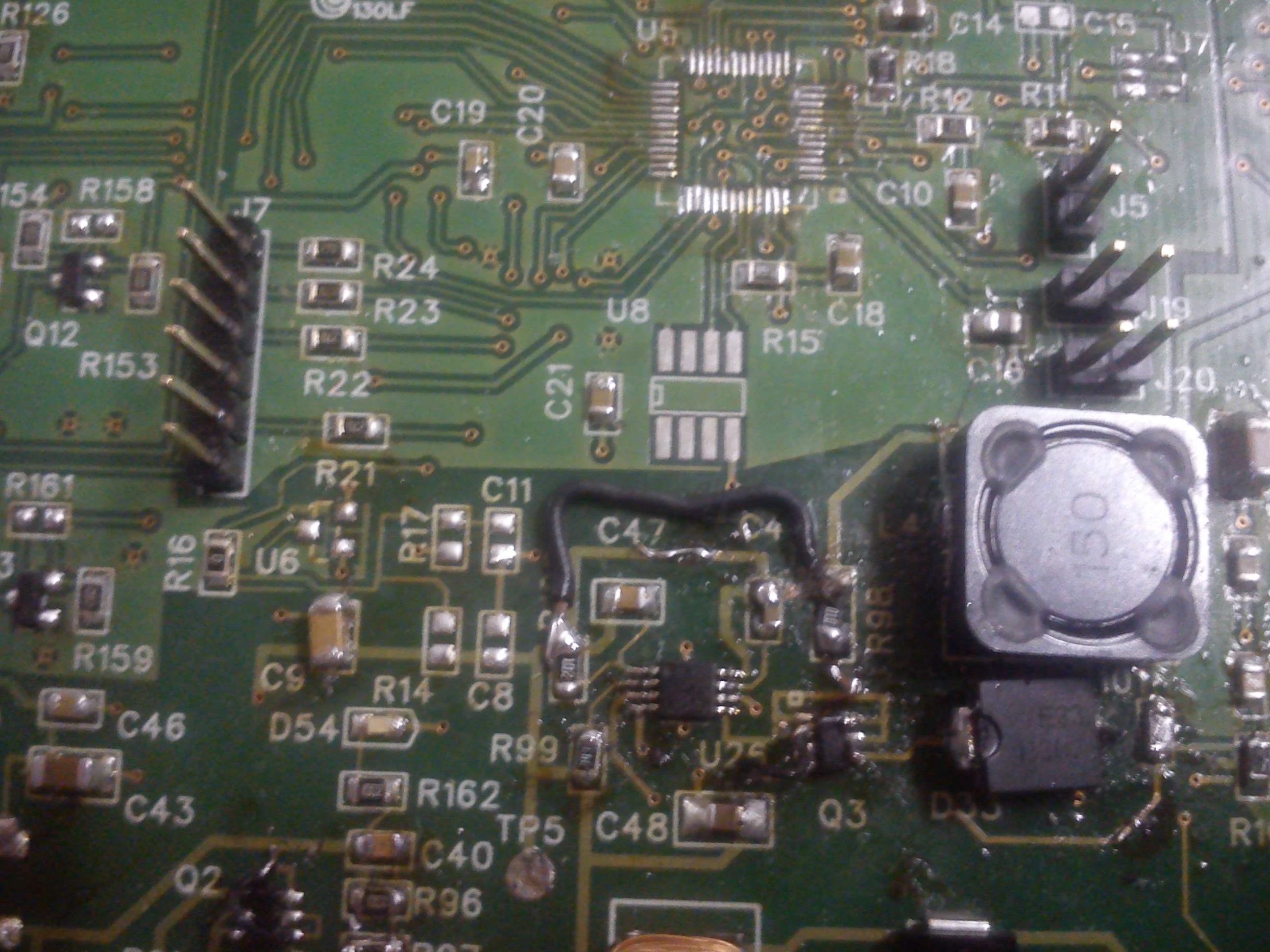
I use Lm25085 with Vin 12V to 32V and Vout 3.3V. In attach the schematic of Webench.
The dc-dc work with Vin 12V to 18V , if Vin > 18V the Vout fall also with low load.
Why? What's the error ?
Bye
I use Lm25085 with Vin 12V to 32V and Vout 3.3V. In attach the schematic of Webench.
The dc-dc work with Vin 12V to 18V , if Vin > 18V the Vout fall also with low load.
Why? What's the error ?
Bye

