This thread has been locked.

If you have a related question, please click the "Ask a related question" button in the top right corner. The newly created question will be automatically linked to this question.

TPS43060 - Undershoot on SW Node and High Drive Gate

Other Parts Discussed in Thread: TPS43060, TPS43060EVM-199, TPS43061

Dear All,

I am using the TPS43060 Boost controller with the following design requirements;

Vin: 24V DC

Vout: 52V DC

Iout (max): 1A

The boost controller has been modelled in webench and the TPS43060EVM-199 evaluation board has been modified as per web bench design recommendations switching at 523kHz , see WEBENCH link below;

http://webench.ti.com/appinfo/webench/scripts/SD2.cgi?ID=153734::power::danielh@pixeltechnologies.com.au

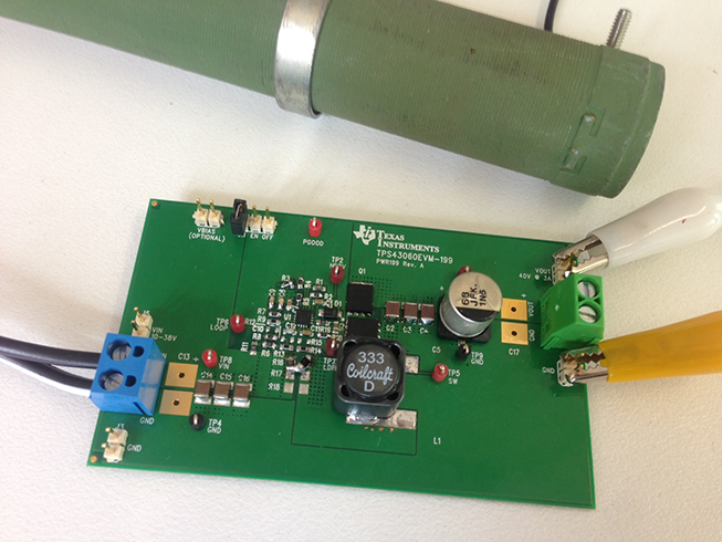
Below is an image of our modified evaluation board.

We are able to achieve 52V DC @ 1A, although we have a 10V plus voltage undershoot below PGND at the SW Node and on the High Gate drive which could potentially damage the boost controller.

How can we eliminate this undershoot, the datasheet specifies driving the low side gate with 4.7R in which we have done, and by adding additional snubber circutry. We have tried the snubber circuitry although this made no difference. 

The BSC340N08NS3 G mosfet selected has a very fast switching characteristics with an rds(ON) of  34mOhms, the 33UH Coil Craft MSS1210-333MEB inductor also has a DCR value of 34mOhm, could this contribute to the undershoot when the low side mosfet initially first turns turns on?

See Low Side, High Side, SW Node and Vout Waveforms below. 

  Low Side Gate Drive

  High Side Gate Drive with 10V plus undershoot

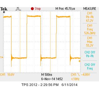
    SW Node with 10V plus undershoot

    Vout with 470mA resistor LOAD.

Would like to add that before changing the mosfet to the BSC340N08NS3G we used the BSC123N08NS3G that came with the evaluation board. This mosfet presented no undershoot and the waveforms were clean. Although we had 80mA of current draw when there was no load, I assume this excess current would be due to the higher gate charge charectestics although as calculated still should not be as high as 80mA. Power efficiency and losses would also prove to be higher so we decided to go for the BSC340N08NS3G which would switch faster and have much better efficiency.

Your help would be kindly appreciated as this is the 3rd attempt to get the booster working before we release the product to the market. Look forward to your feedback.

Kind Regards,

Daniel Haddad

Hardware Design Engineer

Pixel Technologies.

  • I would also like to add that all waveforms shown were taken with a 470mA LOAD and the 10V plus undershoot is also present when no LOAD is connected.

  • A list of component changes made to the evaluation board are as follows:

    Mosfet Q1 and Q2: BSC340N08NS3 G

    Inductor L1: MSS1210-333MEB

    RSENSE: 15mOHM Total (2 x 10mOHM parallel + 1 x 10mOhm series)

    C8: 1NF (COMP)

    C9: 100NF (COMP)

    R7: 2.4K (COMP)

    R5: 110K (Timing 523 kHz)

    R8: 450K (FB)

    R3: 590K (UVLO)

    R4: 40K (UVLO)

    R2: 4.7R (Gate Drive)

    R10: 4.7R (Gate Drive)

    C2,C3,C4: 4.7UF/100V (Cout)

  • Hi Daniel,

    First I would like to check the measurement technique at the SW node. Are you using a tip and barrel measurement or using a very short ground lead by wrapping a wire around the barrel of the probe? It would be good to look at this undershoot with a smaller timescale of around 10 ns/div.

    If the undershoot is there when measuring this way it is most likely caused by the fast switching characteristics of the new MOSFETs and I have seen this before. The first way to reduce it is to use the R10 gate drive resistor but I see you already have one. Try increasing this a bit more to 10 Ohms or maybe 20 Ohms to see if there is any more improvement.

    The next thing to try is adding an RC snubber across the high-side MOSFET.

    You could also try changing to the TPS43061. It has a lower gate drive voltage and should switch the MOSFETs slower. However looking at the Rds(on) versus Vgs curves, the 5.5 V gate drive is probably too low for these MOSFETs though. I haven't checked but I think you might not find any MOSFETs with a high enough Vds voltage and lower Vgs threshold.

    Best Regards,
    Anthony

  • Hi Anthony,

    Yes tip and barrel technique is being used. Thank you for your recommendation to completely eliminate the undershoot R10 needs to be 47R and this has improved.

    See low and high side waveforms below, I have one concern now that the low side gate is charging slower, this will introduce more mosfet power conduction losses due to slew rate decreasing is this correct? 

    Also due to the slew rate on the low side gate drive decreasing is there any chance the high side and low side fet cross conducting and causing a short circuit? 

      low side gate drive with 47R gate resistor

       high side gate drive with 4.7R resistor

    Would it be worth changing the high side gate drive to 47R to match the turn on and turn off time slew rates?

    Your assistance is greatly appreciated.

    Kind Regards,

    Daniel

  • Glad to see the 47R resistor was able to reduce the undershoot. This will add some loss in the low-side MOSFET when switching at higher load currents. Did you happen to measure how much the slew rate changed?

    With this large of a value it would be good to double check the delay between the MOSFETs turning on to make sure there is no risk of cross conduction. It would be easiest to check this by showing both waveforms at the same time and a time scale near 40 ns/div. This way you can check if the delay changed much from the dead-time spec of 65 ns spec. The main transition to look at is from low-side MOSFET off to high-side MOSFET on.

    If you find the dead-time to be significantly reduced balancing the resistors is an option. You could also put a diode in parallel with the 47R to speed up the turn off the low-side MOSFET. As I mentioned above this is the more important transition.

  • Hi Anthony,

    Your help is very much appreciated. We have decided to use a schottky on the low side mosfet to reduce the turn off period slew rate which has helped significantly.

    The gate drive on the low side can be 39R before any undershooting occurs so we decided to settle on this value, and drive the high side with 4.7R.

    Power dissipation is acceptable and we have had the board running for 72 hours now.

    A new PCB design has been released to the manufacturer and we are awaiting prototype units, more measurements will be made with our own PCB design to ensure it performs to spec.

    I will be in touch if we have any more queries and thanks again you have been of great assistance.

    Kind Regards,

    Daniel