This thread has been locked.

If you have a related question, please click the "Ask a related question" button in the top right corner. The newly created question will be automatically linked to this question.

TPS54340-Q1

Other Parts Discussed in Thread: TPS54340-Q1

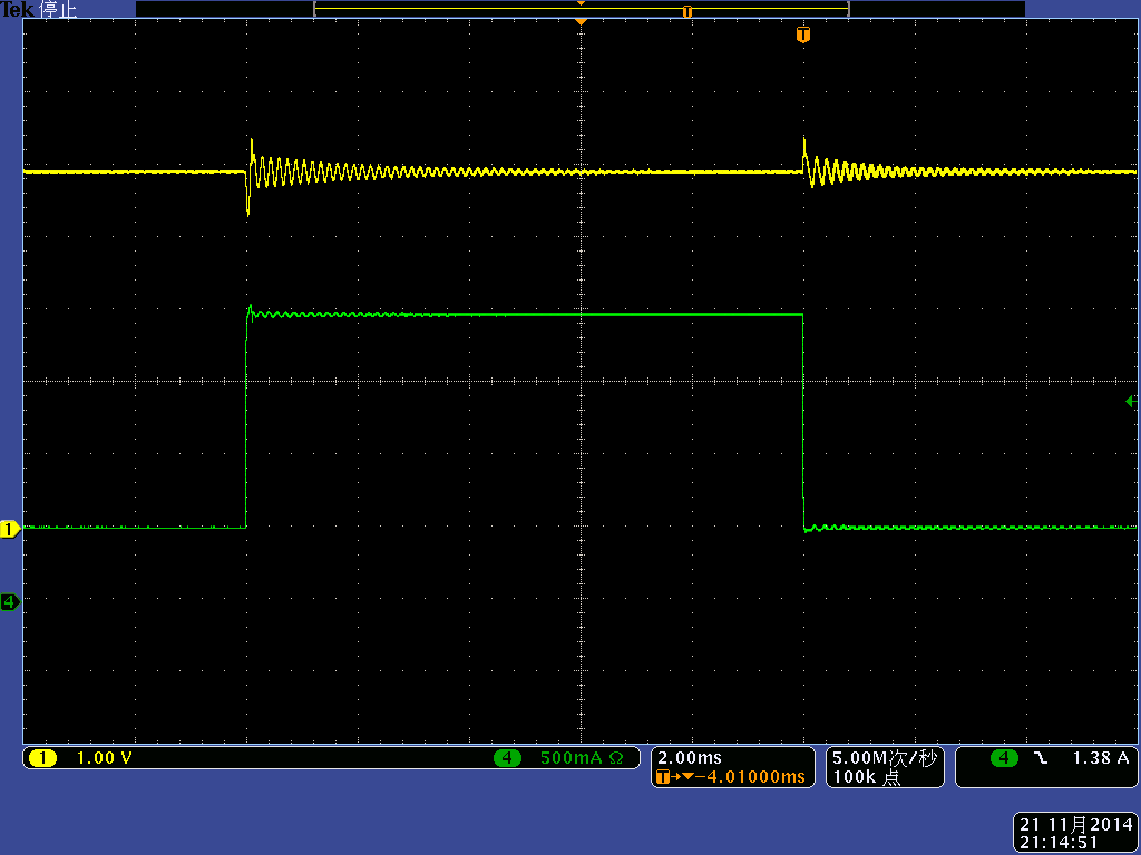
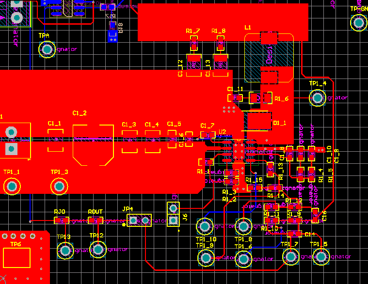
I build up one TPS54340-Q1 board refer to TPS54340-Q1 EVM, during load transient test, found VOUT has some ringing and can hear Inductance whistle. Compared with EVM, remove L2 and L4:

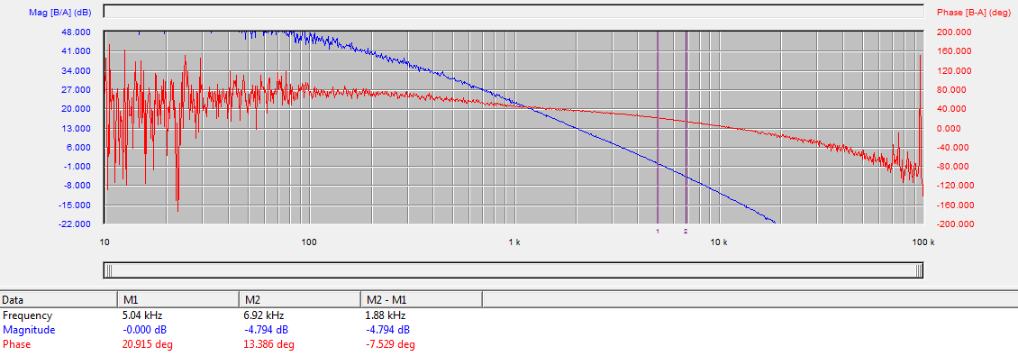
What's function of L2 and L4? Remove L2 and L4 would influence the loop stability? Just roughly test, want to hear some suggestion to move on figuring out the root case, thanks.

  • L2 and L4 are input filters.  They should not greatly affect the loop stability.  If you are pulsing the load at audio frequencies, you may here noise form the inductor.  Can you post your actual schematic and show some waveforms?

  • 2783.Schematic Prints.pdf

    CH1: VOUT, CH4: Load (strep from 0.5A to 2A)

  • That does seem to be quite under damped.  I suspect your phase margin is low.

  • Is this just a modified EVM?  Or did you make your own layout?  The output filter and compensation is the same as the EVM, but your transient waveform is not the same as shown in the users guide.

  • Yes, i build up my-own board because i need do other test, schematic almost keep the same except for the L2 and L4, most of the component like output LC and didoe use the same device with EVM, expect has the same performance.

    Additionally, the output add a USB power switch as the current limit function, and the load add the power switch output, in my understanding, it should very slightly influence the loop.

    Anyway, thanks for your input, i will test the loop phase to see if adequate phase margin.

    One more question, how to decide the input LC filter if used in automotive, power supplied by 12V battery with peak voltage?

  • I'm not sure how the input filter was chosen.  Let me see if I can contact the EVM designer.

  • I re-test the load transient as below, looks bandwidth and phase margin both bad.

    Tried 3 x 47uF output cap and adjust the type II compendation, no siglificant improvement. So has some strange.

    Also here is my layout, because i want to adjust the output voltage, so add several zero resistor in the resistor devider, i am not sure the layout would cause this behavior.

  • Today i test the loop gain: fco=5kHz, phase margin=21degree, but i am not sure why the same compensation, but has different loop gain?

    Additioanlly, use AP Model 300, set AC source is 50mV, AC BW=1kHZ, sweep points=1000,  why so large noise under low frequency?

  • It is not unusual to get noise at one or both ends of the frequency sweep.  You may have to adjust your amplitude, or possibly check your termination.  I can't tell you specifics as I am not familiar with that particular analyzer.

    At any rate you need to adjust the compensation.  You should try for Fco about 50 kHz with 50-60 degrees of PM.

  • Hi Milo,

    How is this going? I worked on the TPS54340-Q1EVM and can help with any remaining questions you have on it. I was out of office for the holidays.

    One thing I noticed reviewing the layout is the output capacitors do not have a very solid connection to the VOUT plane due to the added series resistor. This would add inductance and I wonder if it is enough to affect the loop. Could you try soldering some thick wires from the output capacitors to the VOUT copper plane to try to have a lower inductance connection?

    Also how is this board connected to the transient load? This should also have a low inductance connection through a copper plane.

    Best Regards,
    Anthony