This thread has been locked.

If you have a related question, please click the "Ask a related question" button in the top right corner. The newly created question will be automatically linked to this question.

BQ40z50 DSG pin protection

Other Parts Discussed in Thread: BQ40Z50

Dear all,


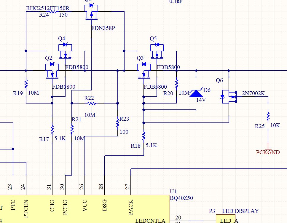
we are developing a BMS based on BQ40Z50.

we've encountered problems in the past related to extreme high current short circuit / over current, for example - 20-30A when usual current is no more than 8A.

the DSG pin allows an absolute of 30V, and actually supplies 26V according to datasheet when discharge FET should close.

what will happen to the chip above this value?

  1. generally speaking: isn't it pretty high voltage considering that LiFePO4 cell can go down as 2.3V (even 2V sometimes), which will create -24V an kill the discharge FET which is typically +-20V Vgs?
    or is this voltage diffrentiate with VSS?
  2. when applying high currents 20-30A its common to see a voltage spike that's adds to Vgs from Faraday law: V=L(dI/dt), it can be a few volts which will bring us to cross the absolute value of 30V on the DSG pin.
    is this taken care of internally in silicon?
    if not, can you suggest a protection application note on the DSG NFET?

    is it enough to place a certain Zener across the 10Mohm resistor? which value would you suggest if so.

best regards,

  • Ran,

    The Abs Max voltage spec on the DSG pin is 32V, so you should not exceed this value. The maximum output voltage from the DSG pin charge pump is 12V, so this should not damage your FET. Remember that the DSG pin output voltage is with respect to the Pack pin, so the DSG pin voltage will drop as the Pack pin voltage drops. (as in a shorted load condition) If the Pack pin is at 5V, then the DSG output voltage should be <17V, and the VGS applied to the FET should be <12V.

    Tom

  • Dear Tom,

    many thanks,

    do you see a need to clamp the excessive voltage of Lorentz Law (not Faraday :-)), that may occur on high current latching?

    regards,

  • You can test it and if the voltage approaches 32V, then a clamp would an option. Also test it with the clamp to make sure that it does not affect the charge pump performance.

  • Dear Tom,

    what helped me before is to change the voltage divider of the DSG pin to reduce the Vgs voltage if needed.
    this is better than experimenting with the Diode and its effect on the latching ability of the IC.

    downside is the larger Iq it creates.

    I guess it is one of those problems you handle if it comes.

    many thanks,

  • Ran,

     The 10 Mohm and 5.1 kohm resistors are not a divider to create the DSG pin voltage. The 10 Mohm is in the circuit to pull the gate to source when the DSG FET is off. You should not change this resistor to a smaller value.

    Tom

  • Tom,

    yes. I know. the resistance has to be very high to keep the FET off when it needs to be off.

    I calm about the design since you said the DSG voltage is roughly the same as pack pin (essentially pack+).

    which means the highest voltage is 16.8V and there is a long way to go up to 30V (pin absolute voltage).

    so why is it written in the datasheet that the CHG, DSG, PCHG, FUSE pins range from 2.2-26V? did you mean it can so as up as that voltage?

  • The DSG pin voltage will be approximaty the Pack voltage plus 12V when the FET is turned on. The 12V is from the charge pump. The DSG will reach 20 to 30V, but the VGS of the FET should not exceed the charge pump voltage, 12V.

  • in this case,

    every long enough spike or voltage addition can damage the IC or reset it.

    since ~16.4V is the initial voltage of a full 4 cell Li Ion battery, + 12V is easily 28.4V.


    I attached a schematic for you to see, where I think the Zener should be (at least I'll prepare foot print of it).

    as you said: I'm not sure what will happen if the zener is on, the excessive voltage will have to go back to the charge pump probably.

     have you ever dealt with this kind of concern from other designers?

  • Will the control of the Mosfet work without the 10MOhm resistance? Is it possible to use those Mosfets in the Pack- path?

  • The FETs will still be able to be turned on or off without the 10M resistors, but it is good design practice to have them there since it ensures the FETs will shut off in case power to the gauge is lost.

    The FETs must be in the Pack+ path. The bq40z50 will not be able to drive them on or off if they are in the Pack- path.