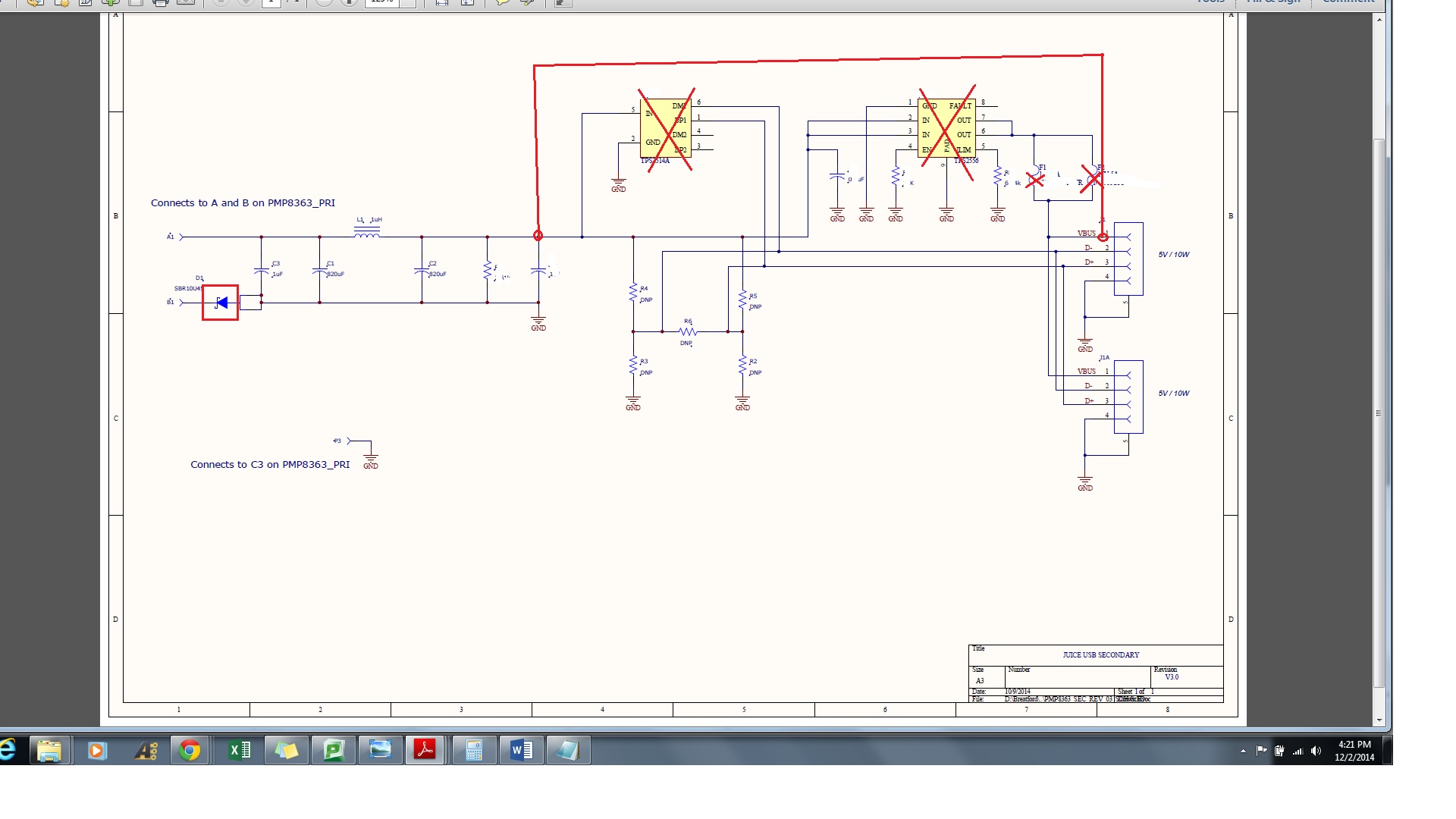
Hi TI Team, I need your help. Please respond with detailed answers. Appreciate it 1. Why was UCC28700DBV used in case of 2.1A design? whereas UCC is used for 2.0A design? Is there any difference between those 2 ICs? 2. For 2.1A design CBC/NTC pin is connected to Gnd via a 10K resistor, but for 2A design it says R1(DNP)? Would you please clarify? 3. In case of 2.1A design, in the secondary side you have used U1-TPS2511DGN but not for 2A design. Is there any reason for that? 4. Currently for both 2A & 2.1A designs R2-R6 are DNP. When are you going to use them and to what value? Few questions regarding using your IC UCC28710 for a 5V/2.4A(12W) design instead of 5V/2A(10W). Can I use the same schematic as used for 5V/2A design of yours for the 12W by tweaking the below? 1. Increase f-sw(switching or freq) or decrease t-sw.-->How Do I Achieve That in This IC?? 2. By reducing Rcs ( as in the IC spec)?? 3. Any other parameters? 4. Can I use the same Transformer as RTLI 1067 or 1061 for this new 12W designing (including thermal performance at room temp) which I'm trying to do? Thanks a lot. Arin