Dear Power Supply Boffins,
Before I bother you with my question I would like to point out that phase one of my business plan allocates a large chunk of cash towards engaging a firm of professionals to do the PCB layout and design. All I am trying to do is ensure that my early investors don't receive a letter stating that due to an unfortunate oversight the project is a bust. So long and thanks for all the fish.
Also, the device is a wearable and forms only part of a much larger system. It is critical the device be available as close to 24/7 as possible and therefore discharged batteries will be swapped for fully charged ones when required. The device cannot even be left charging overnight.
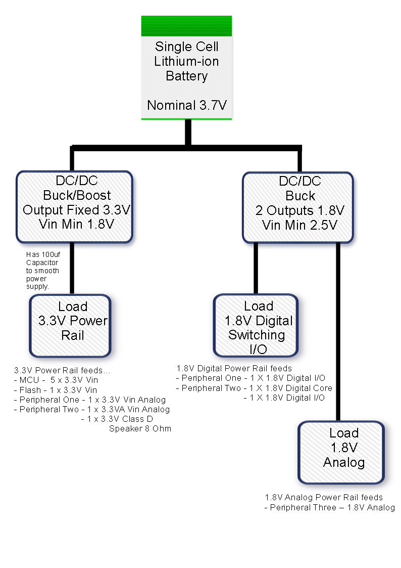
Having satisfied myself that a cellphone-type Lithium-ion battery will be suitable for the device (post http://e2e.ti.com/support/wireless_connectivity/f/968/p/386215/1362355.aspx#1362355) and that the TPS63001DRCR 3.3 V buck/boost with a Murata 100 µF Capacitor (GRM31CR60J107ME39L 6.3V 20% X5R) will PROBABLY allow me to use a single supply for both digital and analog (with appropriate bypass capacitors as per reference designs) I am left with the following question.
I have a number of components which require 1.8V supplies, both for analog and also digital I/O.
I have considered the following possibilities...
(a) Two batteries. Ruled out because of size constraints and because the device needs to monitor the battery and inform the wearer with time to spare that a discharged battery needs replacing. Can't have one battery running flat and rendering the device inoperable.
(b) A buck/boost that has multiple outputs with a built in LDO for the 1.8 V supply. Ruled out because the only such regulators have a quiescent current requirement that is too high at around 15 mA.
(c) A voltage divider. Ruled out because to obtain a sufficiently stable output voltage, the output current must either be stable or limited to an appropriately small percentage of the divider's input current.
(d) An LDO that is separate from the buck/boost (don't know the implications really). Ruled out because to output 1.8V an LDO linear regulator needs to have an input voltage of 2.8V minimum, which is higher than the minimum voltage that the buck/boost requires to still output 3.3V (which is 1.8V).
(e) An LDO that has as it's input the 3.3 V from the buck/boost and lowers it to the required 1.8V. As the only possibility I haven't ruled out it seems a a waste to dissipate 1.5 V as heat.
Is there an option I haven't come across in my research?
Any input would be greatly appreciated.