This thread has been locked.

If you have a related question, please click the "Ask a related question" button in the top right corner. The newly created question will be automatically linked to this question.

TPS62133 Fails On Load Transient

Other Parts Discussed in Thread: TPS62133

Hi,

I'm trying to diagnose a frequent failure of a TPS62133-based circuit. Testing shows that the circuit causes the switcher to fail frequently, but not always (i.e. there are some instances that appear to survive forever.

I have narrows it down to a sudden load transient when the input is 12V or more. This condition often occurs as result of switching on a load that does not have proper in-rush current limiting. My understanding of the datasheet is that the '33 should be protected against load over-current and short-to-ground.

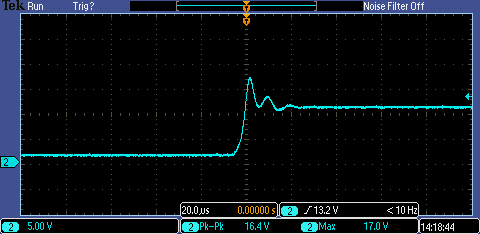
Here is a capture of the input and output of the switcher during such a failure. In this case, I'm switching about 0.5ohm load (which is expected to cause the current limiting to activate, but not to fail the switcher).

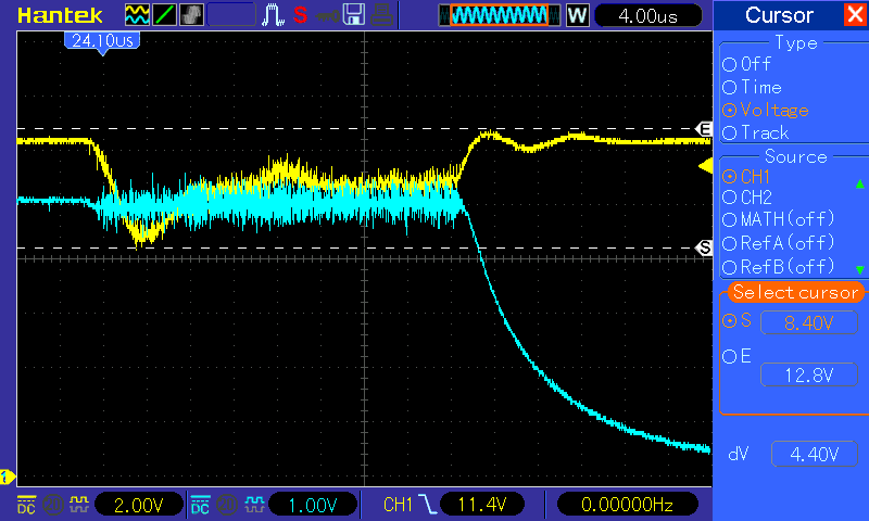
Yellow is input (nominal 12V) and cyan is output. It is evident that  the Vin ratings are maintained and the failure occurs after around 30[us].

Here is the relevant piece of the schematic:

And the layout is very similar to the reference:

(input from the right, output to the left, the output capacitor C6 is on the top (missing its outline in this image).

We have seen this failure on tens of units from two different manufacturers, all assembled automatically.

Unfortunately, many of those units have been shipped to customers, and we are now trying to figure out the right fix as soon as possible.

Thanks!

  • Does this only happen when the load transient is seen with 12Vin or higher? i.e. it does not occur when Vin is 11V? What sort of input source is it? It has a fairly high impedance to drop that much in your waveform.

    Could you supply the part numbers for each cap and the inductor?

    As well, is it possible to add the inductor current onto the waveform?

    Finally, I see that there is a trace on the bottom layer from the via on the VOS pin going up to another via. Where does this go and why? This pin is very sensitive, so I would try testing with this trace cut.
  • Thanks!

    Chris Glaser said:
    Does this only happen when the load transient is seen with 12Vin or higher? i.e. it does not occur when Vin is 11V? What sort of input source is it? It has a fairly high impedance to drop that much in your waveform.


    I've increased the input voltage gradually and have only been able to make it fail at about 12V. Input source is a bench Power supply. The high impedence is mostly a result of long wires and connectors. This was done deliberately in order to simulate worst case inrush ringing although it is irrelevant in this test.

    Chris Glaser said:
    Could you supply the part numbers for each cap and the inductor?


    C6: LMK212BJ106KG-T
    C10: TAJA106K016RNJ
    L2: VLC5045T-3R3N

    Chris Glaser said:
    As well, is it possible to add the inductor current onto the waveform?


    Unfortunately, I don't have a good way to measure it with my available tools and without being too intrusive.

    Chris Glaser said:
    Finally, I see that there is a trace on the bottom layer from the via on the VOS pin going up to another via. Where does this go and why? This pin is very sensitive, so I would try testing with this trace cut.

    It only goes to a 2mA LED. Seems to be pretty insignificant unless I'm overlooking something.
  • Thanks for sending your BOM. You used a 3 Ohm ESR tantalum cap for the input cap. This is not allowed for any modern SMPS, as its impedance is far too high. Per the D/S, this must be a ceramic cap.

    In the 1206 case size, there are many 22 uF and 10uF ceramics to choose from. Try with one of these and see if you still see failures.
  • Apologies, I posted the part number of the wrong part.
    The input capacitor is C11 and its part number is umk325c7106mm-t. It is indeed a low ESR ceramic, as required.
  • Ah, ok. It seems to be an ok cap with ok DC bias performance.

    Is your testing at room temperature? Do you have a current probe available?

    Can you explain in a little more detail what you mean when you say the IC fails? Vout clearly goes to 0V, but if the load is removed and/or the IC restarted, does Vout come back up? Does the IC get hot without a load after this test?

    Could you take a waveform of Vin on the TPS62133 as the 12V is applied to your system?
  • Testing is at room temp.

    I do not have a current probe available, but could probably get one. Probing the inductor current would be hard and very intrusive but probing the input and/or output current should be quite easy.

    When I say fails, I mean becomes and open circuit irrecoverably. It does not get hot nor consume any current, but fails to output anything long  after the load has been removed and the input cycled.

    Attaching a Vin waveform for an earlier test. Note that there is a simple protection circuit on the input that doesn't kick in in this case, but would clamp the input if it exceeds about 18V. We have verified that even in the presence of higher input inductance and input voltage the voltage is correctly clamped and never exceeds the maximum rating of 20V.

  • A spike that high on Vin seems a little worrisome for fear that tolerances, etc. could make it higher. It would be worth trying to add more input capacitance on the PCB (like a 100uF tantalum) and see if that spike magnitude is reduced. Then, with the reduced spike, see if it still fails during the load transient.

    Otherwise, yes, I would need a waveform of Vin, Vout, SW, and the inductor current at around 5 usec/div when it fails. Measuring the inductor current isn't intrusive electrically. All the graphs in the datasheet were done this way: remove the inductor and solder it to the SW node on one terminal; then put a wire from the other terminal to Vout and clamp the current probe there.
  • Chris Glaser said:
    A spike that high on Vin seems a little worrisome for fear that tolerances, etc. could make it higher. It would be worth trying to add more input capacitance on the PCB (like a 100uF tantalum) and see if that spike magnitude is reduced. Then, with the reduced spike, see if it still fails during the load transient.

    As I mentioned, there's a protection circuit that hard-clamps around 19V. As you can see from my original graphs, there was no spike recorded during the failure. I have done a lot of testing with toggling the input and have not managed to damage the TPS, so I don't think this is a concern in itself (unless you think it may suggest something else).

    Chris Glaser said:

    Otherwise, yes, I would need a waveform of Vin, Vout, SW, and the inductor current at around 5 usec/div when it fails. Measuring the inductor current isn't intrusive electrically. All the graphs in the datasheet were done this way: remove the inductor and solder it to the SW node on one terminal; then put a wire from the other terminal to Vout and clamp the current probe there.

    Intrusive in the sense of having a substantial impact on the layout and adding resistance between the inductor and the output cap, which is inside the feedback loop. I'm waiting for replacement parts to arrive and I'll try to produce those graphs. What are we expecting to see? What might be the possible causes for failure given what we know? Is it possible for me to send a few samples to TI for an engineer to look at?

  • I'm not suggesting that spin the PCB to add the wire. Just do it by hand. The minimal added resistance is not important.

    This is the standard waveform needed for debugging. It will tell us what the IC doing, where the currents are going, etc.

    If you have a local FAE, he or she would be an excellent resource to debug with you on the bench.