This thread has been locked.

If you have a related question, please click the "Ask a related question" button in the top right corner. The newly created question will be automatically linked to this question.

TPS73512 problem with the output voltage

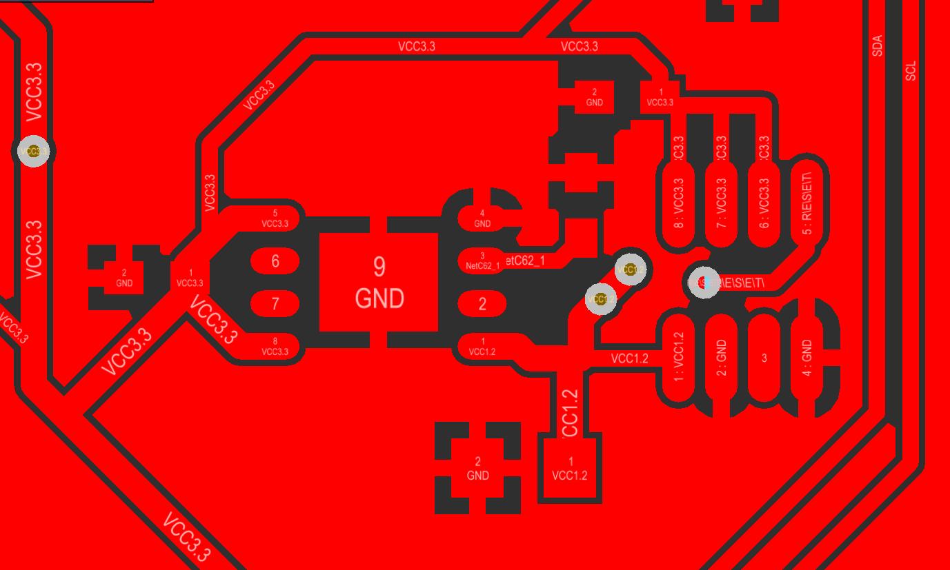
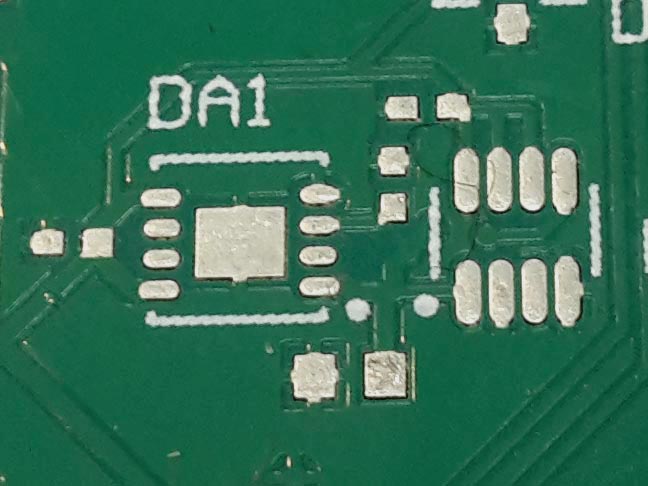
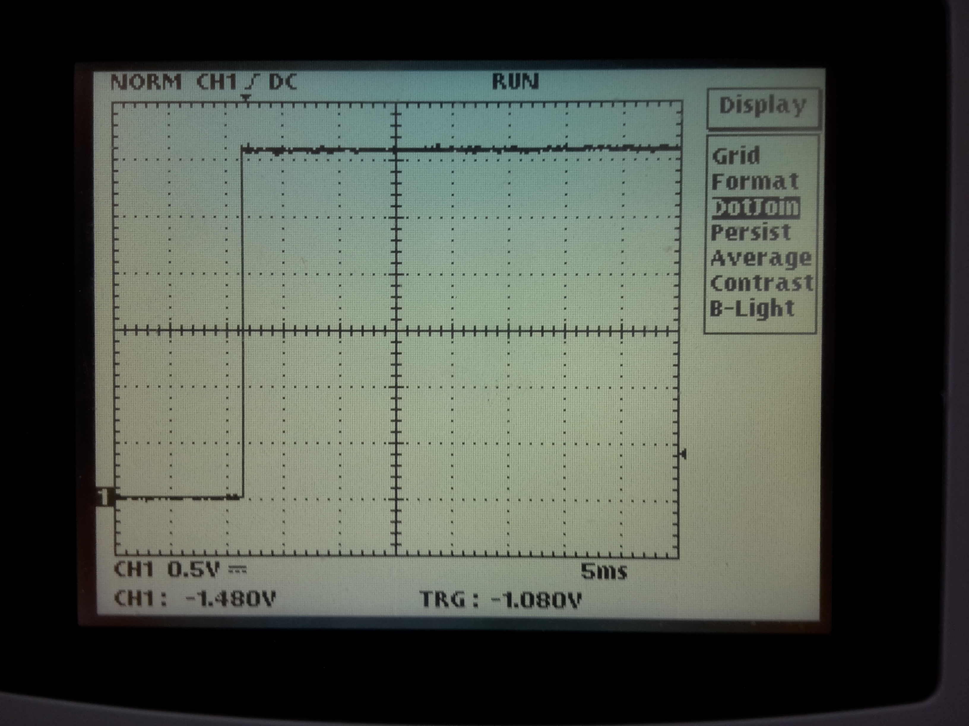
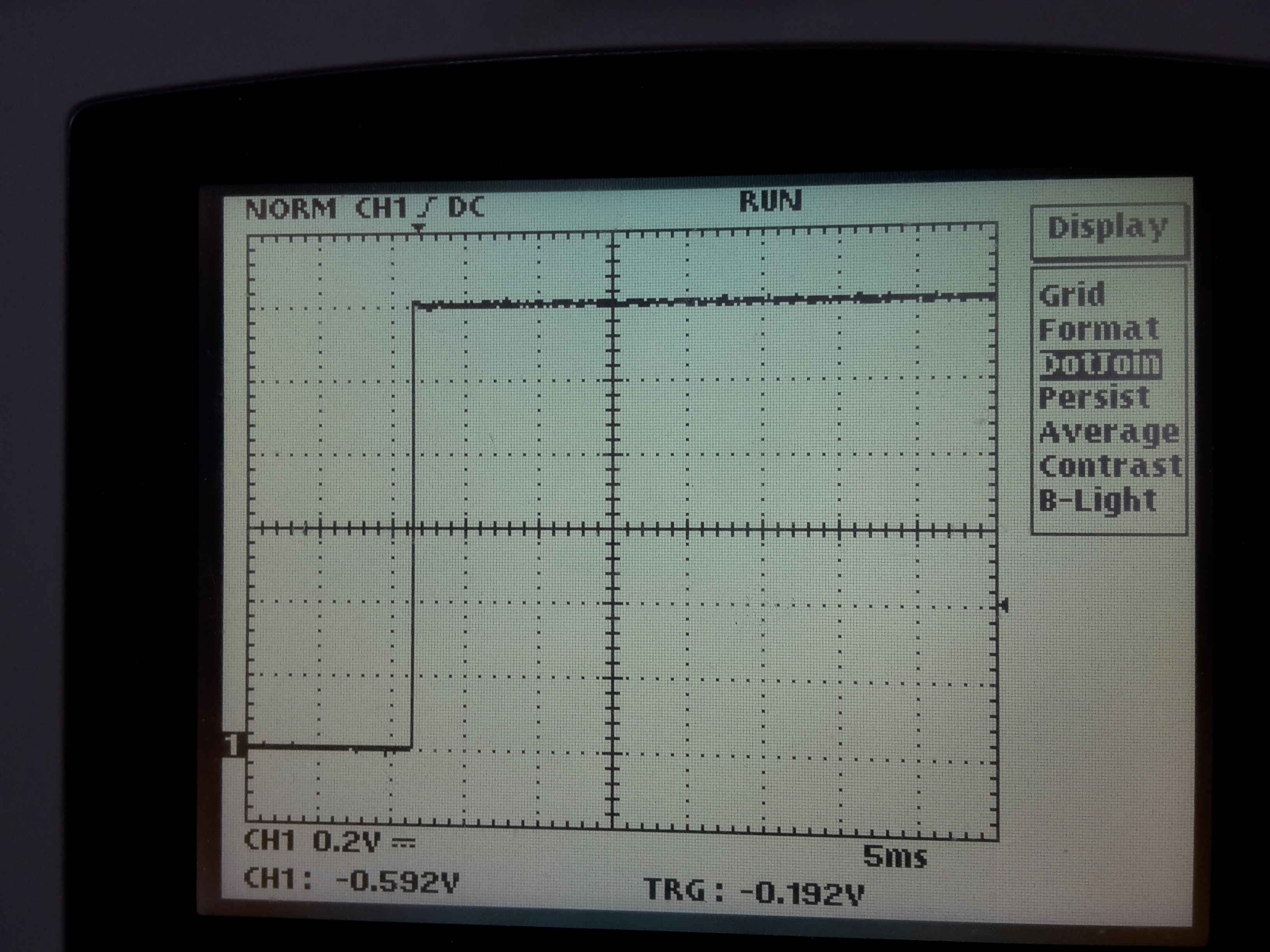
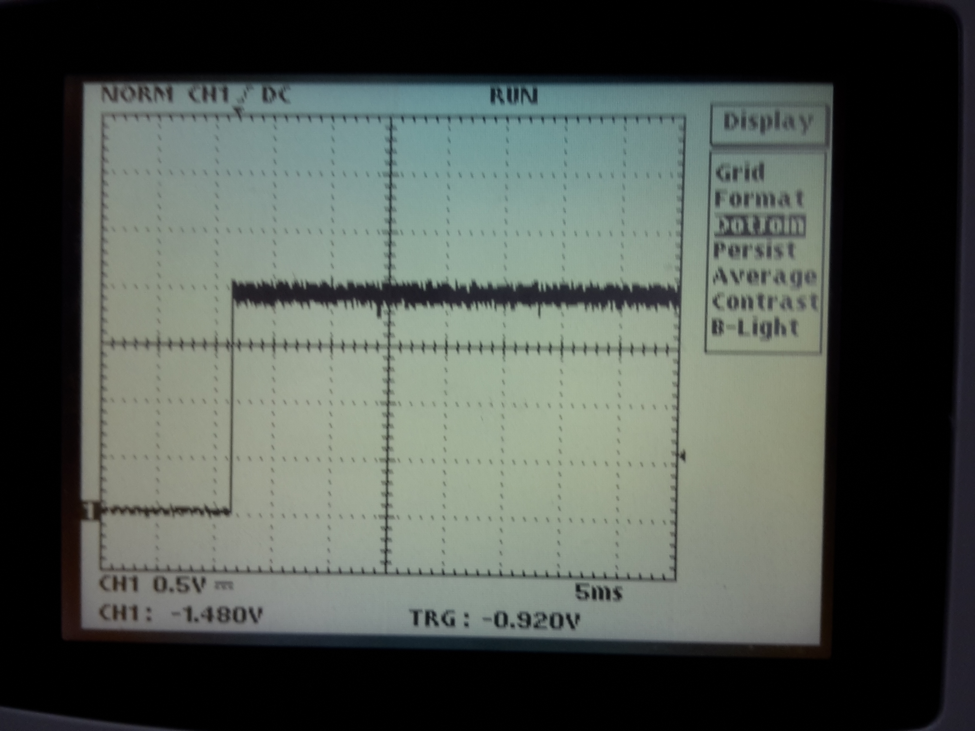
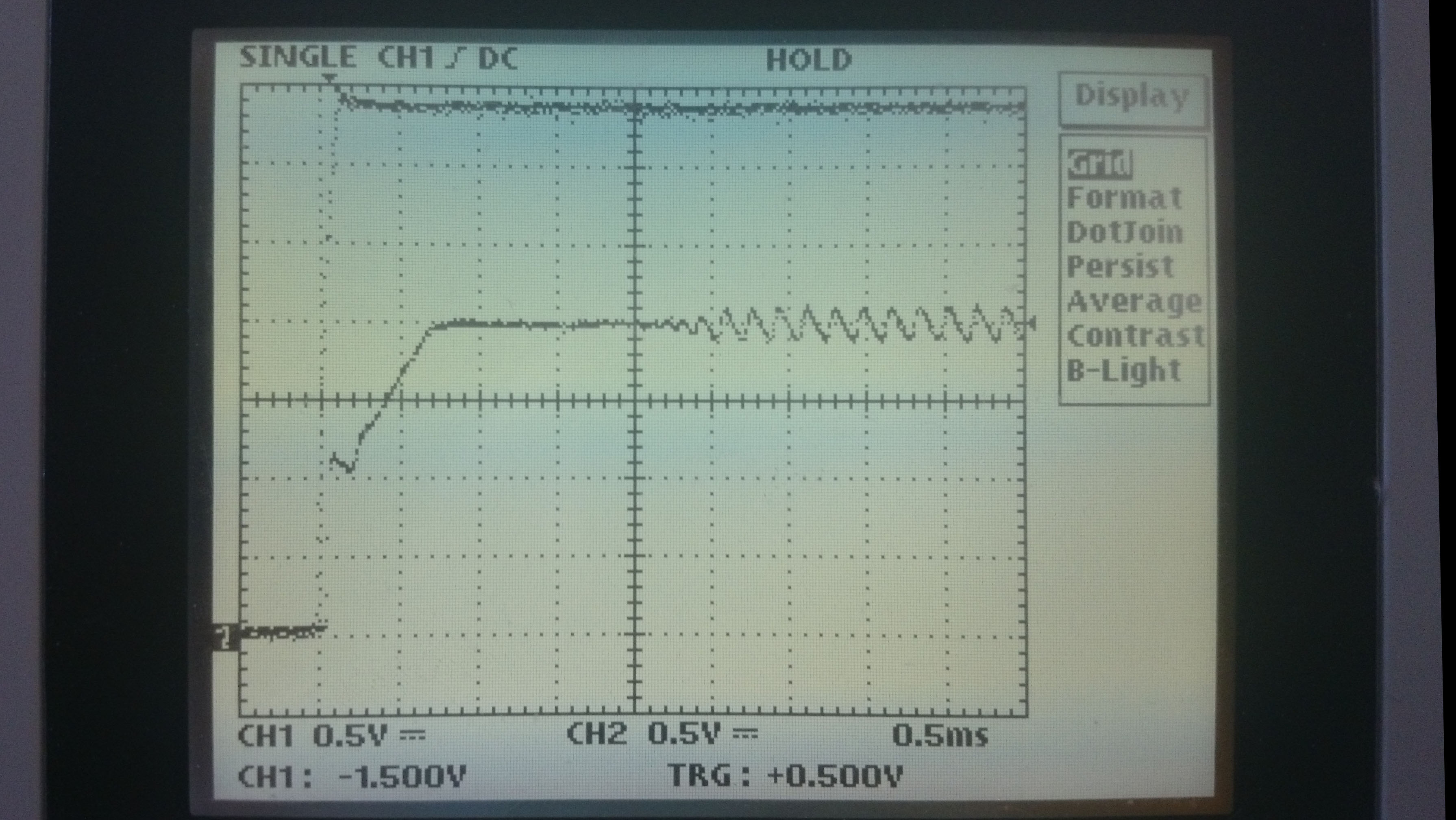
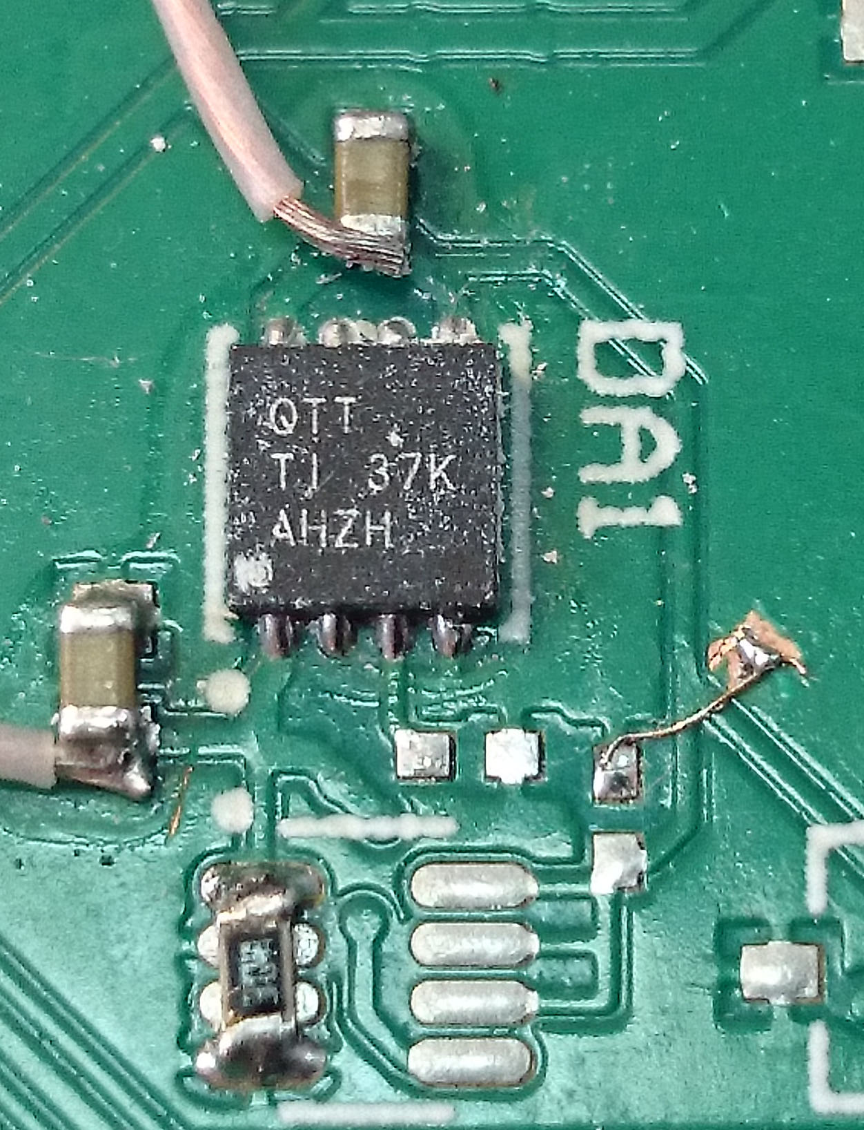
Hello all, I have a problem. Recently began testing a device where applicable TPS73512, and found that the output voltage of 3V no load and 1.8V under load. Documentation output voltage should be 1.2V. Check the voltage at the output of the filter, which should be 1V, 1.8V appeared there too.

What am I doing wrong? The signals are correct input voltage 3.3V, GND is connected. Capacitor at the input 30 uF and 10 uF at the output,

  • Hi Nord,

    In order to help with the debug, could you please provide a schematic and scope shot of Vin, Vout, and Ven?

    Is there anything downstream on your board that could be biasing the output?

    Very Respectfully,

    Ryan

  • Hi, Ryan.

    After reading your response, I began to test these devices and found that one of the three was working. All three chips were from the same batch and from one tape.

    I rule out the possibility of damage to the chip during soldering.

    Now the answers to your questions:

    Ryan Eslinger said:
    could you please provide a schematic

    1. Connection diagram is used similar to that shown in the Datasheet.

    Ryan Eslinger said:
    Is there anything downstream on your board that could be biasing the output?

    2. After the chip is only Supervisor and the core FPGA

    Ryan Eslinger said:
    scope shot of Vin, Vout, and Ven

    Images: 

    1. PCB model 

    2. PCB real 

    3. Vin and Ven (connect together to 3.3v) 

    4. Vout load 200 ohm working chip   and not working chip 

    5. V filter (pin #3) working chip   and not working chip 

  • Hi Nord,

    From your PCB model I am unable to see where the input capacitor GND connects to the GND for the rest of the device. Is there a connection outside of the snip you shared?

    Very Respectfully,
    Ryan
  • Hi Ryan.

    Although I'm sure that all signals GND are connected together, I set the jumper to make sure that it does not help.

    On the test board is assembled only a voltage converter to avoid damaging another new FPGA. 200 ohm load. Capacity of condensers - 10 uF. 

    With this configuration were obtained all photos that I post earlier. Of course except jumper, which recently soldered.

  • Hi Nord,

    Thanks for double checking the ground connection. It looks like in the "not working" scope shots there is oscillation. Could you zoom in on this? Also if possible, could you have the input in the same scope shot?

    Very Respectfully,
    Ryan
  • Hi Ryan

    I forgot to do DotJoin, but I think that it is not necessary.

  • Hi Nord,

    Could you please confirm the topside marking of the device?

    Very Respectfully,
    Ryan
  • Hi Ryan.

    According to the datasheet marking coincide with TPS73512.