This thread has been locked.

If you have a related question, please click the "Ask a related question" button in the top right corner. The newly created question will be automatically linked to this question.

TPS65563A question and schematic review

Other Parts Discussed in Thread: TPS65563A

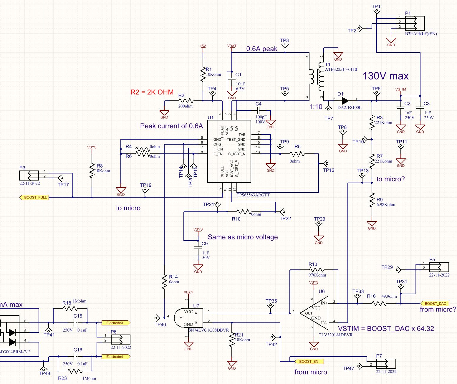
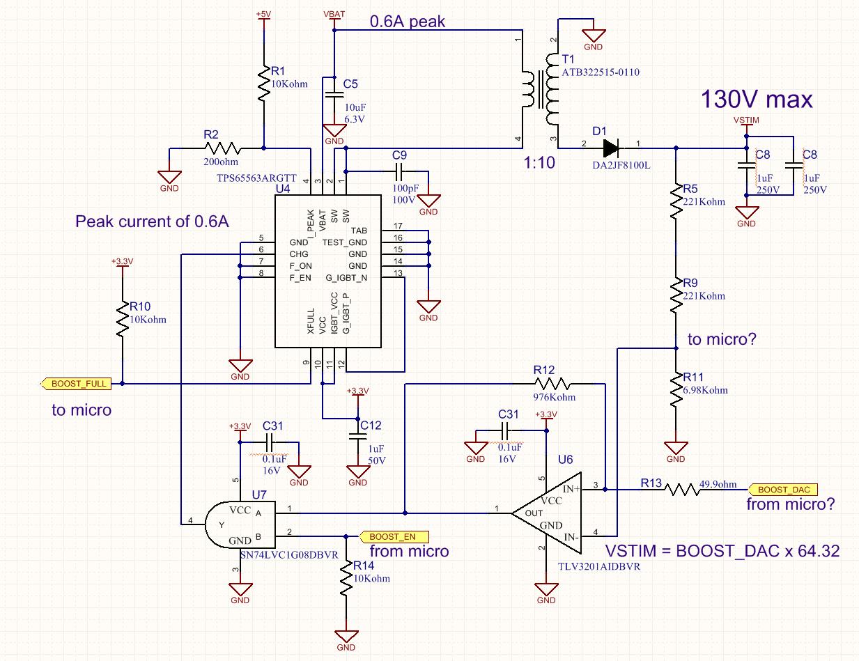
We’re using the TI TPS65563A on the Novus project. Basically the operation is to charge the output caps to a max. 130V then discharge this output

to an electrode set. This delivers a current thru the electrode (capacitively coupled electrodes) to stimulate the muscle. Recover than by maintaining the 130V maximum set output voltage (worst case). Based on how much current is required for stimulation (100mA maximum) the output voltage is set.

Thus the allowing the output voltage to change and notify the uC when the voltage supply is at the set point (charge full) this is a nice part.


That said it has an internal IGBT that is used to fire a xenon tube flash. We are not using a flash bulb so tying the IGBT is require (?) or may it be left floating?

Or is tying the F_EN and F_ON low enough to safely disable the IGBT? Does all of the connections on this part appear correct for our use?

Thanks - Jeff

Thanks

  • Hello Jonathan,

    I think your circuit will work as you expected.
    You can leave its IGBT function unsed; leave G_IGBT_P and G_IGBT_N outputs open.
    As you may have noticed that this device can stop charging when Vout reaches to its target of 29V at primary side. If you use 1:10 transformer, 290V (minus Vf of diode in precise). You may use 1:4 or 1:4.5 transformer. But your using a comparator gives more accurate Vout detection.

    best regards,
    Masashi
  • Masashi, I'm working with Jonathan on this circuit.  Can you answer a couple more questions?

    1.  In the datasheet there is no mention of connecting the center pad to GND.  I've looked at SLVA318 as well and didn't find any note.  It simply states that it should be attached to a copper thermal pad.  Can you confirm that it should be left unconnected to any other net?  

    2.  I made a couple of modifications to the circuit above.  Only difference is I removed R5 and changed R2 = 2k ohm so I have 0.8V at the Ipeak pin.

    This is what I’m noticing – I have my Boost enable (BOOST_EN) pin so the charge pin (CHG) gets a low going high to start the charging process.  It starts and stops so the voltage doesn’t ramp up. I’m expecting the voltage to ramp till the U6 comparator toggles and changes the CHG pin too low to stop the charge process.  This is how the data sheet explains it.  How this is working is as long as I cycle low-high-low-high ect… on the CHG pin the output voltage never increases and when I stop this cycle the output voltage drops quickly.  What am I missing? Also the XFULL signal stay high the whole time. (VSYS) is the +3.3V from the logic supply.


    Could you help identify the issue?

  • Hi Mike,

    thanks for  your update.

    Ans-1

    the reasonable connection is this thermal pad to GND or a broad thermal plane "floating".

    Ans-2

    it seems like this is expected discharge by R3-R7-R9.
    At 100V, these 3 resistors in series draw 0.21mA.
    This current is out from C2+C3 = 2uF.
      i = c * dv / dt
      0.21mA = 2uF x dv / dt
    when we think about 5V drop (dv = 5)
      0.21mA = 2uF x 5V / dt
      dt = 2uF x 5V / 0.21mA
      dt = 48ms
    Of course, as Vout decrease discharging current will be smaller but, to me, what you see is R3-R7-R9 discharing from the output capacitor.

    For this purpose (preventing sense resistor to discharge), we have primary sensing feature with this device.

    best regards,

    Masashi

  • Masashi - The 3 resistors in series are 221k + 221k+6.98k = 448.9k so at 100V / 448.9k = 222uA But the output is not staying charged with no other load added. I have to pulse the charge pin constantly to keep the output at 130V. The data sheet leads me to believe the charge pin to the charge pump requires just a high to charge and low to shut off. Is this true then why would I need to pulse the charge pin? I did measure the resistance at the output across the 2 - 1uF caps and measure 448.6k ohm thus only the feedback path is the load. Thoughts? - Jeff

  • Hi Jeff,

    So I think my calculation is right.  Please review it again.

    best regards,
    Masashi