This thread has been locked.

If you have a related question, please click the "Ask a related question" button in the top right corner. The newly created question will be automatically linked to this question.

TPS23754 bode plot fail

Other Parts Discussed in Thread: TL431

Dear sir,

  I have the circuit that followed attached schematic to design but change output cap to MLCC.

(C18 change to 100uF x3 MLCC, C19 change to 100uF x9 MLCC)

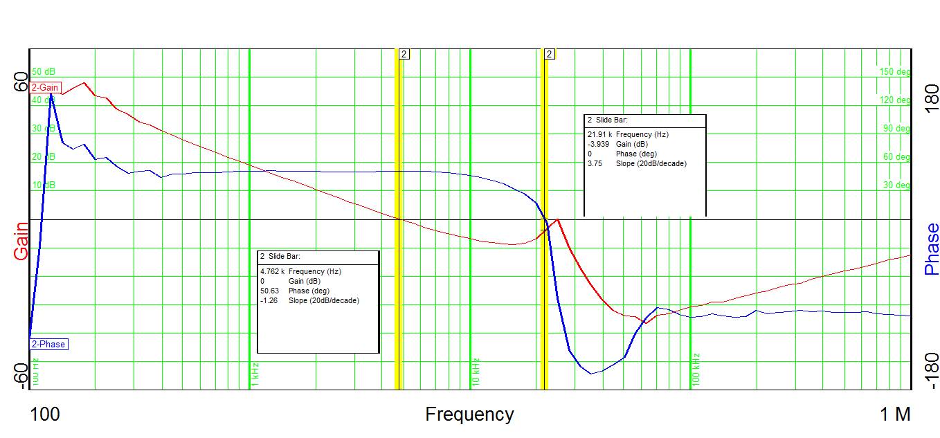
But now we can't pass bode plot gain margin to 10dB.

Would you help to provide any comments to improve bode plot? By the way, we can't use oc-con or AL-cap because this may need 7 or 8 year life cycle,

we need to keep MLCC output cap.


slva475.pdf

  • Hello ShihChin,

    The replacement of the the 330 uF Al Electrolytic capacitor with low Resr ceramic capacitors reduces the loop gain phase margin in your bode plot. To add an additional phase margin boost, the flyback output filter must be re-analyzed and a new compensation circuit that accounts for the loss of the Resr must be designed. The tl431 error amplifier has a zero formed by C31 and R29. The output of the opto U3 also has a compensation network that needs to be re-designed. This network consists of R25 and c29 that forms a pole at R25*C29. There is also a series network of R24 and C30 that forms a pole and zero. So you have to figure out where these poles and zeros are and then either change the values of the Rs and Cs or add another network. For instance, Tl431 could be configured as a Type III error amp to get more gain boost in the bode plot.

    Chuck

  • Hi ShihChin Lo,Everything Chuck says is true.
    A 'quick and dirty' solution is to place a 1ohm resistor in series with each of your 100uF MLCC capacitors. This gives them an ESR like the E-caps and hence your Bode plot should be the same as if E-caps had been used. There are many other ways to solve the problem, but they will require greater understanding of your objectives.
    Best Regards Joe Leisten
  • Hi Joe & Chuck,

      Thanks for your reply.

    So do you have any suggestion value or do you have calculation tool to calculate this value?

    Do you ever design flyback or forward topology with all MLCC? If yes would you help to send to me for reference?

    Thanks.

  • ShihChin,

    Sorry for the late response. The design of an isolated DC DC compensation is not trivial. I usually take two or three days and I have a lot of experience.

    Here are some steps you need to take to re-design the compensation loop.

    You need to develop an AC average SPICE model  of the converter. 

    Read "Fundamentals of Power Electronics" by RW Erickson and "Switch-Mode Power Supplies" by Christopher Basso.

    (Make sure you get the errata sheets for both books.)

    From the AC average SPICE model you can obtain the open loop frequency response. -I use the books I referenced above to determine the SPICE model

    First you run the SPICE simulation with no compensation. 

    From the loop response of the uncompensated network you can determine the amount of gain and phase shift required to obtain a stable converter.

    From the aforementioned references you can find the R and C values required to design your compensation network. Basso's book has a good section on the TL431 and how to use it as error amplifier. 

    Once you have determined the compensation network and simulated it on SPICE (I use LTSpice. You can use whatever SPICE simulator you prefer.) you need to test it with frequency response analyzer, FRA, like the Bode 100.

    If you don't have access to an FRA, there are other techniques you can use to test the loop gain response. You can google the internet using loop gain response test with oscilloscope and a link to a nice application note AN 1889 will result.

    Hope this helps.

    Chuck