Other Parts Discussed in Thread: TPS63001
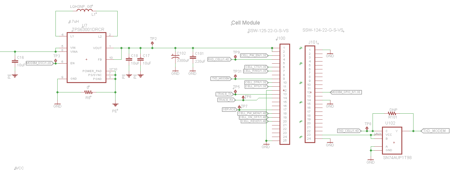
- The TPS63001's sole purpose on my board is to supply 3.3v, <1A typ. to a cell phone module.
- I am seeing an output variation as low as 3.27v at no-load to light load at ambient temperature and a further decrease beyond 300mA out.
- Output voltage continued to decrease as temperature dropped. At -30C my output was as low as 3.1v.
- For consistent testing load was simulated to provide peak and average current required by the modem.
- Input voltage: 4-cell, 3.6v Lithium ion battery. Our custom battery pack does not fall below 3.3v at -40C.
- The enable pin is controlled via the micro from a separate 3.3v rail.
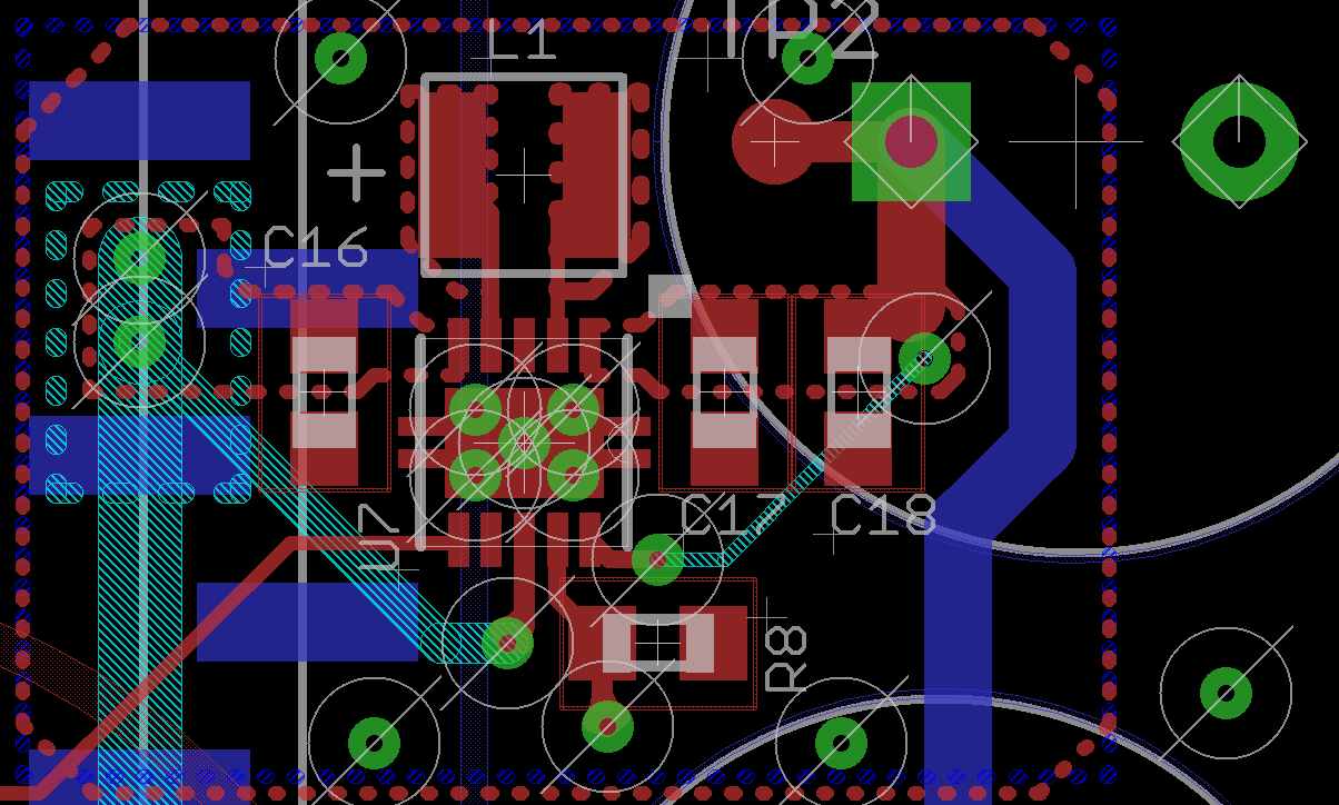
- PGND and GND were tied at the GND pin via a zero ohm resistor. The resistor was placed encase a ferrite bead would have been necessary to filter noise from the PGND plane.
- Inductor is 4.7uH Murata chip recommended on the TPS63001 data sheet.
- Pads on the bottom plane are not tied connected.
- Thermals were turned off.
- Could you evaluate my design giving pointers at where I might start to rectify my discrepancy?