This thread has been locked.

If you have a related question, please click the "Ask a related question" button in the top right corner. The newly created question will be automatically linked to this question.

Is there an inherent body diode in GaN power FETs? If so, what is the V/I curve for that?

Other Parts Discussed in Thread: LMG5200

Is there an inherent body diode in GaN power FETs? If so, what is the V/I curve for that?

  • GaN does not have a body diode similar to Si MOSFETs as the conduction takes place due to the formation of the 2DEG. When current tries to free-wheel through the GaN device while it is off, it will first flow through the output capacitance, CDS. This will produce a negative VDS, and eventually a positive VGD. The device will turn on and current can flow through the channel once the source-drain voltage is greater than (VTH-VGS).
    VSD > VTH − VGS
    This implies that the third quadrant drop typically will be larger than Si MOSFETs (as shown in Pg. 7) of the technology guide www.ti.com/.../lmg5200.pdf
    Care should be taken to minimize the dead time to get the best possible system efficiency for hard switched DC/DC converters.
    Regards,
    Narendra
  • hello Narendra Mehta,
    Can you explane why this phenomenon happens detailedly.
  • I'll try explaining it another way too see if that helps.

    There is no body diode in the GaN FET, so to conduct in the reverse 3rd quadrant mode the device has to turn on. Since the voltage on the gate is applied with respect to the source, when a voltage is applied to the source a voltage is also applied to the gate. When current attempts to flow through the device from the source to the drain, the output capacitors will charge up and generate a voltage. When the voltage exceeds the threshold the device will turn on and current will flow through the channel of the device.

    On an IV curve this action looks very similar to a diode, but please keep in mind that the threshold voltage of the FET is typically higher than body didoes that power Si FETs typically have so the dead time should be minimized to reduce the additional loss.
  • what is "in the 3rd quadrant mode"?

    "When current attempts to flow through the device from the source to the drain",which mosfet did you refer to,switch mosfet or sync mosfet?

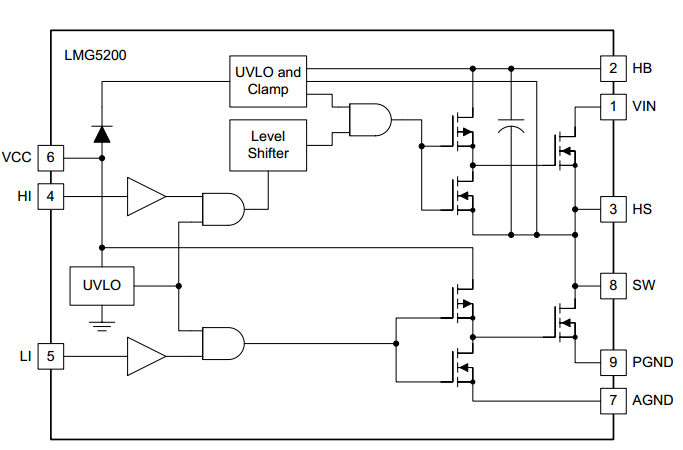
    can you explain the reason using  the picture below?

  • 3rd quadrant mode refers to when current flows from the source to the drain of a FET.  This is in reference to the typical IV curve of FETs that have Vds on the x axis and Ids on the y axis, since the plots that refer to the mode of operation at this point occur in the 3rd quadrant of the graph.  Typically for power FETs this current would conduct through the inherent PN junction diode that is present, but the GaN FETs that are in the LMG5200 do not have this structure so the FET 3rd quadrant operation occurs instead.

    Since this is a function of the 3 terminal GaN FET device this will occur when you apply a voltage to either FETs in the LMG5200.  The bottom FET will conduct in 3rd quadrant mode when you apply a voltage or attempt to source current from PGND to SW and the top FET will conduct in 3rd quadrant mode when you apply a voltage or attempt to source current from SW to Vin.

  • and there is a negetive voltage on Vsw during the dead time ,why it occurs
  • It depends on the application whether it will occur or not.

    For example the top FET will conduct in 3rd quadrant mode when the LMG5200 is configured to operate as a synchronous boost converter. Since the top FET is operating as a synchronous FET when the bottom FET is turned off the inductor current freewheels from source to drain (SW to VIN) through the top FET. Until the top FET is turned on this current causes the top FET to operate in 3rd quadrant mode.

    If you have any questions about synchronous FET operation this app note explains the basics well www.ti.com/.../snva595.pdf
  • i used it for sync buck,can you explain why there is a negetive voltage on Vsw during dead time?And this phenomenon still occurs in TI's LMG5200EVM
  • The top device would not conduct in 3rd quadrant mode and Vsw will not go negative when the LMG5200 is operated in a constant current mode buck converter. Only the bottom device will operate in 3rd quadrant mode in this case.

    Earlier I was describing basic device operation earlier in a matter where the VIN, SW and PGND are not connected to a larger circuit. Depending on the topology that the LMG5200 is used in will effect which, or even if the GaN FETs in the LMG5200 will operate in 3rd quadrant mode.
  • Hello Kissn Liu
    I am Hangzhou analog FAE support LSD. Can I have your contact information that we can talk about it more effective? emai or phone both is ok.
    My email is X-zhu@ti.com.
    Thank you.
  • If I absolutely needed a body diode, would it be ok to connect diodes from VIN to SW, and from SW to PGND?
  • Installing diodes if using the circuit in a hard-switched technique will cause a reduction in efficiency and is therefore not advised. The diodes will add their junction capacitance in parallel with the parasitic output capacitance of the FET, which will add to the capacities switching losses.

    Generally, when selecting GaN , efficiency improvements are possible as a result of reduced parasitic capacitances. Adding extra components would negate that benefit.

    To avoid or minimize the 3rd quadrant conduction the solution is to time the control circuitry correctly by minimizing dead time between synchronous switches, in which case these losses will be minimal (and significantly smaller than what would result by adding didoes).

    That said, if using a zero voltage switching technique, and wanted to add those diodes, they would have to be installed follows: top FET one diode cathode connected to Vin, anode to SW. And the bottom diode with cathode connected to SW and anode to PGND.

    Even in this case optimal efficiency is achieved by reducing the dead time rather than adding the extra components.
  • GaN HEMTs do not have an intrinsic body diode. The devices exhibit different characteristics depending on the gate voltage. A negative gate voltage is added to the reverse voltage drop “Vf” and hence increase the reverse conduction loss.

    Further information regarding reverse conduction of GaN-HEMTs can be found at:
    www.gansystems.com/faq-e-mode-hemts.php
    epc-co.com/.../eGaNFETCharacteristics.aspx


    But there is a simple solution shown in the paper: Integrated reverse-diodes for GaN-HEMT structures :
    ieeexplore.ieee.org/.../abs_all.jsp
    However this approach is not available as a product jet.