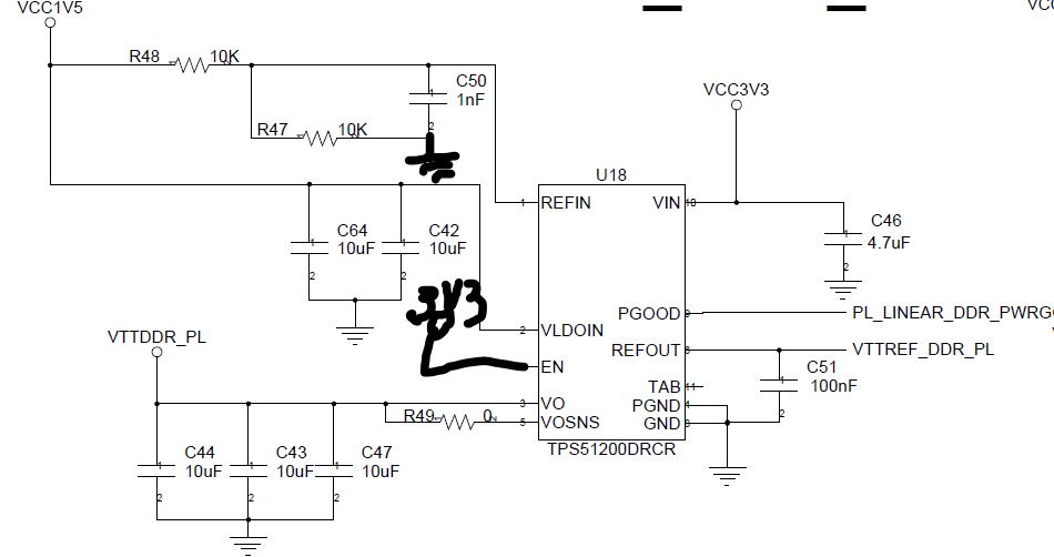
I have two TPS51200 circuits that are identically designed as shown in the schematic snapshot below. In the original layout the resistor divider for the REFIN was left ungrounded and the EN pin was left unconnected. The board has been modified as shown. The PGOOD pin is pulled up to 3.3V through a 10k resistor at the input of a buffer that is driving an LED in another location on the schematic. Also, the thermal vias on the in the bottom pad were left out.
I am getting mixed results from the circuits. One one circuit, I am seeing right at 0.749V at REFIN, but I am getting about 0.82V at VO and REF_OUT. The other circuit does not seem to behave at all. The REFIN value is also around 0.75V, but I am seeing results that swing between 0.06V and about 0.3V (the change is very slow, almost as if there is some sort of capacitive chare/discharge happening).
Is it possible that the part that does not behave at all simply needs to be replaced?
And for the part that seems to be near normal function, is it possible that the lack of thermal vias in the power pad is causing incorrect values (which may be the case on the other part as well)?
After extended periods of the board being powered the parts are not warm to the touch, but we are currently in a very early troubleshooting phase and the DDR3 chips are not being exercised as of yet.