Hi All,
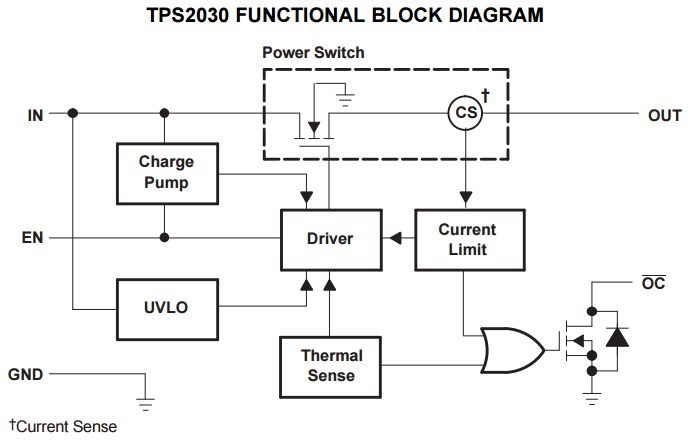
I confirmed the block diagram but it has no body diode on internal power FET. I believe that actually it has body diode and the reverse current will be flowed from OUT to IN if the bias will be applied on OUT with no input. Is my understanding correct?
I understand the absolute maximum rating of OUT is VI(IN) + 0.3V, so the bias higher than it is cause of damage.
Best Regards,
Sonoki / Japan Disty


