This thread has been locked.

If you have a related question, please click the "Ask a related question" button in the top right corner. The newly created question will be automatically linked to this question.

Why does not my PCB design for TPS7A4700 and TPS7A3301 work?

Hello,

 I have designed the two devices output to be +15.8V and -15.2 V respectively. While when Vin<~15V, Vout~=Vin, when Vin is approaching 15V, the devices start to burn. I have checked the connection, I believe they are correct as suggested. While there might be some issues in the thermal pad connection and I have used vias to connect the capacitors, I believe there might be other reasons for my failure. Could anyone have any idea? Thanks!


Best,
Min

  • Hi Min,

    What is your load current and final input voltage?

    Regards,
    David
  • I did not use any load, just use a voltmeter to measure the output voltage. I have gradually increase the input voltage from 0 to 16 V, the when Vin<13V, Vout is similar to Vin, when further increases, Vout is zero or the device burns. I can see the sparks. I have use the same set up for the evaluation board, while Vout=15.8V when Vin=16.4~20V.
  • Hi Min,

    That is certainly odd - could you post your schematic and layout?

    Regards,
    David
  • Hi David,

    Please see my schematic

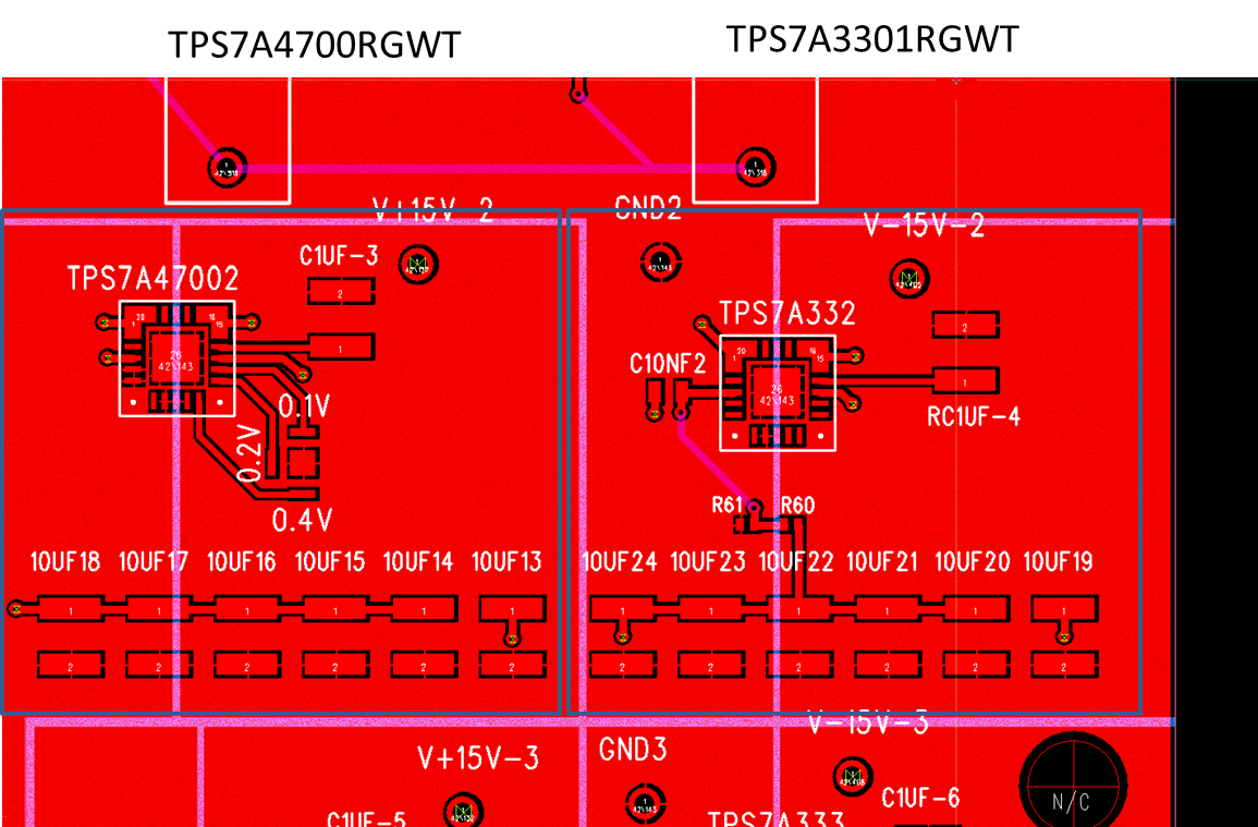
    my PCB layout as followed, my PCB has 4 layers, top and bottom are ground, 2nd is power plane (can see the lines divide Vin+, Vin-, Vout+, Vout-), 3 is a trace layer

    And my real PCB looks like follows, I solder by hand, thus did not do a good job in soldering the thermal sink in the middle, while I feed this should not be the reason to cause my problem. For TPS7A3301, i use R1=620kOhm, R2=51kOhm, in order to get Vout~=-15.5V

    I have the same problem for these two devices, the when |Vin| approaches 15 V, |Vout| stops to increase and the device burns. I can see sparks if I do not use helium gas to cool it while operating. I just use voltmeter to measure the output, so no load current.

    Hope you can help me to figure out. Thanks!


    Best,
    Min

  • in case the capacitor values are not clear in the picture, please see this one.

  • Hi Min,

    You could have a short through the thermal pad, or some solder flux residue in between your thermal pad and your ground that is causing some type of coupling. What is the current draw from your supply as you increase Vin?

    Regards,
    David
  • Hi david, as Vin<~14V, current is zero. As Vin towards 15V and above, the device burns and the current is large which appears to be a short circuit. I am wondering if that is the reason you mentioned, why it is good when Vin is small and only occurs when Vin is approaching the point I want? I also see some sentence in the data sheet says
    "10.1 Layout Guidelines
    For best overall performance, all circuit components are recommended to be located on the same side of the
    circuit board and as near as practical to the respective LDO pin connections. Ground return connections to the
    input and output capacitor, and to the LDO ground pin, must also be as close to each other as possible and
    connected by a wide, component-side, copper surface. The use of vias and long traces to create LDO circuit
    connections is strongly discouraged and negatively affects system performance. This grounding and layout
    scheme minimizes inductive parasitics and thereby reduces load-current transients, minimizes noise, and
    increases circuit stability."
    I have used vias and 4 layers in my design. I am wondering is this device that critical in this requirement? Thanks!
    PS. as you also mentioned one concern, I'll send it out to the company to solder the components and test again.
  • Hi Min,

    The layout you have is good for thermals, but may cause some issues as it looks like you viaed to your input and output capacitance - this typically can lead to oscillations in certain conditions.

    For your failure condition it seems like you have a marginal short that breaks down at a higher voltages.

    Regards,
    David
  • Hi David,


    I have asked a company to solder the devices for me and now they are working. It seems that the short comes from that the ground plane in the bottom of device is so close to the other pads. The chips should be positioned very critical to avoid shorts after soldering in my design. And I think Pin 1/20 and Pin 15/16 should not be soldered together in a single large pad. Solder mask should be put on top that.
    Since I have failed many times to solder manually. I want to ask if there are any other equivalent packages of the chips? There is a KC package for the TPS7A3301 while I do not find any other package for TPS7A4700. Do you have any more information?

    Another question if I have designed the output of the regulators to be +/- 15V, I am wondering the max input voltage we can apply. And also the optimal input voltage range for this? I have tested 21 or 22 V is fine. But will it degrade the functionality if the input and output voltage difference is that large for a long time? What if the input voltage is 25V above? will it damage the device?

    Thanks very much!


    Best,

    Min