This thread has been locked.

If you have a related question, please click the "Ask a related question" button in the top right corner. The newly created question will be automatically linked to this question.

TPS61291 and LP5907 for low power applications

Other Parts Discussed in Thread: TPS61291, TPS63000, TPS63030, TPS63036, TPS61220, LP5907, MSP430FR5969, TPS62740, LP2985, TPS61098

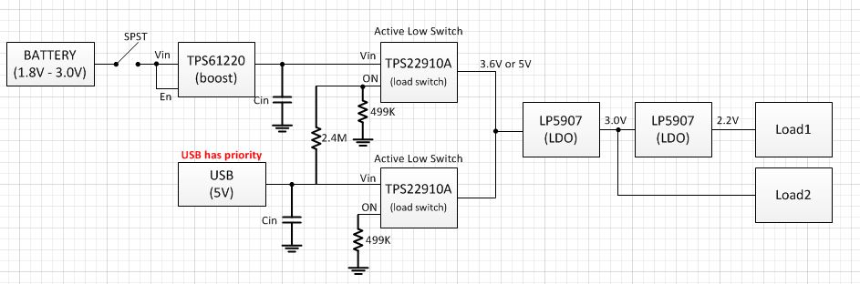
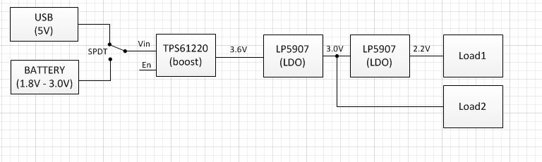
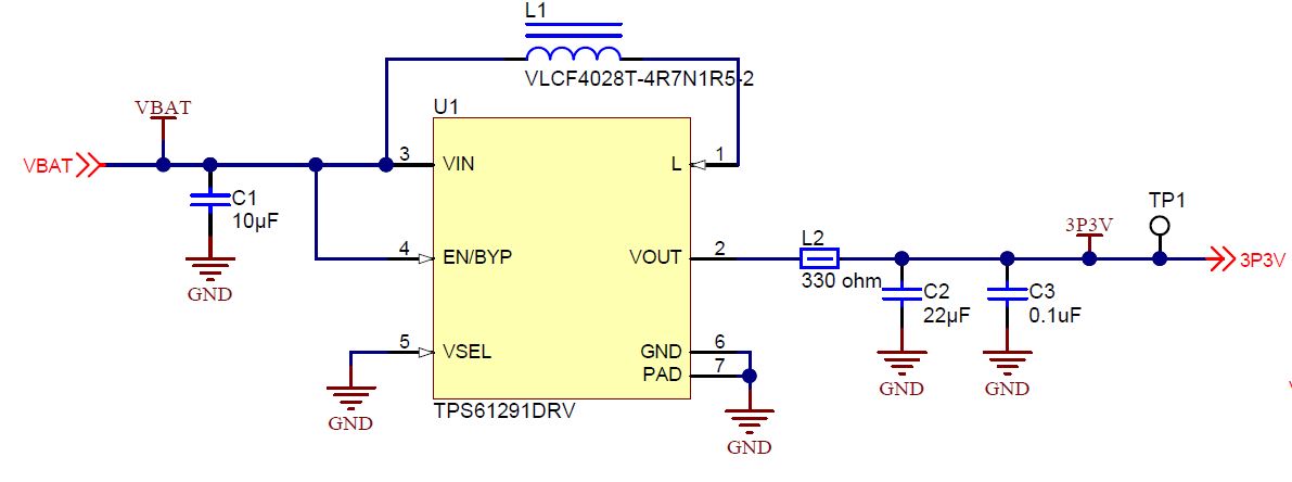
I am creating a design for low power applications. The power supply can be either 2AA batteries (1.8V to 3.0V) or USB power (5V). I need 3.0V and 2.2V to power the devices on my board. The bypass pin will be connected to the MSP430. The current needed at the output of the TPS61291 is no more than 75mA.

Is there a more efficient way or a better product to use for USB and battery output switching? Iq is very important for our application.

  • When supplied with 5V, the TPS61291 will pass this through to the output and you will get 5V there. I don't think that is acceptable for your application.

    A TPS630xx buck-boost converter could take either the USB or battery input and give a regulated output voltage. These would be the TPS63000, TPS63030, or TPS63036. The current consumption at light or no load is relatively high for these devices.

    Do you need 3V and 2.2V or will one voltage do? What type of application is it? Knowing these items, we can create a better power tree for you.
  • Hi Chris:

    Thanks for the response. The two inputs are USB and 2AA batteries. When the input is USB, we do not care about the power consumption, it's only a concern when the battery is applied. The USB is for just backup. I was looking into the TPS61291 to go from the battery supply (1.8V - 3V) to 3.3V, but I am concerned about if there is enough input margin for the LP5907. I am looking at the TPS61220, which is similar in Iq, but has a wider output voltage range.

    I wanted to have 3.0V and 2.2V outputs because I will be running the MSP430FR5969 on the 2.2V at a low operating frequency (to limit power consumption), and then everything else would run off the 3.0V since most of the devices have a minimum operating voltage of 2.7V. I am looking at no more than 75-100mA current combined.

    The application is a capacitive-based proximity sensing wakeup for thermostat applications. The design will stay in sleep mode and wake up periodically to detect a user hand, if no hand, it will go back to sleep, if there is a hand, then the display will turn on and display temperature and humidity data. Then there will be cap touch buttons to enable different modes to adjust temperature, etc...If the cap touch buttons are not touched after a certain amount of time, the entire thing will go back to sleep.

    The diagram below shows what I was thinking about. The power multiplexing circuit is nice so that if both supplies are plugged in, only the USB gets priority.

    This was my initial thought without the power multiplexer scheme, but how would I control the EN of the boost in a low power way so that when the USB is plugged it, it goes low, and when the battery is plugged in, it goes high.

    Any other suggestions would definitely help, especially for this low power application!

    Thanks

    -David Wang

    Capacitive Sensing Applications

  • Also what are some of the advantages/disadvantages of using a buck/boost compared to just a regular boost with the configurations above?
  • You can move this internal if you need to.

    A buck-boost would be 1 IC required to get your 3V from both inputs. The batteries could be diode OR'd with the USB port to make a Vin to the buck-boost. Then, a stepdown is needed to get 2.2V.

    You might consider running everything at a common voltage--3V or 2.7V. This would reduce the number of regulators and thus cost.

    I'm not sure what is special about that LDO. A buck converter would be far more efficient. TPS62740 is a great one to use. Here's a blog (which refers to a paper) where I describe it in a thermostat: e2e.ti.com/.../smart-thermostats-connect-to-the-iot-enabled-by-power-management

    I think you should keep TPS61291 and connect it directly to your batteries. Control its enable from the MSP430. Boost to 3V. Connect your USB port through an LDO to the same 3V net. A voltage divider from the USB 5V to the MSP430 would allow it to detect if a USB voltage is present. If it is, then turn off the boost. Or you could use an architecture like what you have drawn where the power sources are combined at the beginning and an LDO needed afterwards. This would be less efficient when running on batteries. In either configuration, you will need to figure out how to prevent current from the USB port from flowing into the batteries. The TPS61220 might work for this, those load switches, or some reverse polarity FETs/diodes to prevent backwards battery insertion.

    Then, from your 3V rail, you use TPS62740 to get 2.2V.
  • Thanks for the suggestion and information.

    The reason why I chose that LDO is because it's has a very low Iq but also a very high PSRR, which is important for our capacitive sensing device (clean power supply). If not, there would be issues with possible noise on the supply lines affecting our capacitance measurements. We were using the LP2985, but the LP5907 is cheaper, lower power, and better noise rejection.

    The TPS62740 looks good, I suppose that it should be clean enough for the MSP430?
  • Yes, probably any DC/DC is ok for a digital device.
  • Hi Chris:

    So I decided to go with the tPS61291. I was running some webench sims with different load conditions. Most of the inductor selections come up with a 3.9uH. The datasheet has 3.3uH. I designed a board with a 4.7uH to try and cut down the voltage ripple more, but it seems like it may be instable. I am looking at my output on my board and it shows ~4.25V as the output. I have an input of ~2.1V and set the boost to be fixed at 3.3V.

    Can you confirm what the issue is?

    Thanks

    -David

  • You need to place the ferrite bead after the output caps.
  • Could you explain what the effect is? Since the L is right off of the VOUT, is that effect LC low pass filter somehow affecting the output?
  • hi David
    for a boost converter, the output capacitor must be placed directly with VOUT pin and GND pin because the current flowing though the VOUT pin changes in step.

    thanks
    Jasper Li
  • hi David
    we are designing TPS61098, lower quiescent current (400nA), so better light load efficiency. you can email me if you interest in this boost converter.

    thanks
    Jasper Li