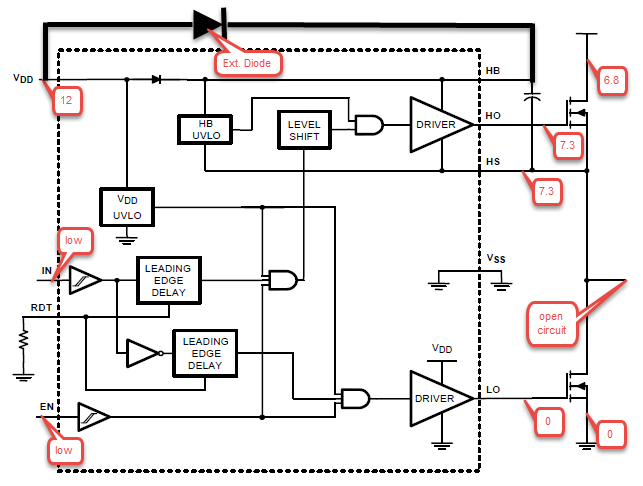
Half bridge with LM5105, open circuit at junction of MOSFETs, With enable pin low, Vdd=12V, no HV upper MOSFET. Upper MOSFET source and gate = 7.3V. Upper MOSFET drain = 6.8V. Please see image of the circuit schematic.
The puzzle we are trying to solve: Why is 7.3 V present on HS, and therefore on HO? We believe that a disabled device should cause HO=HS, but in some cases, we see HS = 7.3 V = HO. This causes our BIT system to fail. In cases where our system does not fail, HS = 2.7 V = HO. In either circumstance, real operation appears to be unaffected. And why would a disabled driver with HV and load open, show any voltage at HS and HO other than something near 0?
DC brushed motor application.
Two half bridges each motor.
Each half bridge is as described earlier. LM5105 driver with a dual MOSFET. Additional external bootstrap diode.
The motor connection on each half bridge is connected to ground with a 57.6K resistor (I neglected to show this earlier).
4 motor drives , 8 half bridges.
The problem is associated with our Built-In Test (BIT) system. We have had no known problems with real functionality, even in the case where the issue arises.
BIT for the motor drives cannot be run with the motor high power applied due to the nature of the system power up and the BIT routine. BIT in this case uses a low-current “trickle” supply derived from the +12V supply (same as that supply used by the drivers) connected to the motor power bus. During BIT, alternate low and high side MOSFETS of the full bridge are turned on, and we observe the collapse of this low-current trickle supply. If the motor is open or a MOSFET does not turn on, or if we have a shorted MOSFET, we can observe those cases.
The BIT trickle supply looks like the following from +12V to motor high power: Resistor, zener, blocking diode. When the high power comes up, the blocking diode is reversed biased. Otherwise with the motor bus supply disconnected, we supply a bit of current to the motor bus for BIT from +12V. At the beginning of motor drive BIT, we check the motor bus voltage, and it must be within a particular range. Working boards have the motor bus voltage around 5 V, about what simulation predicts. Our problem is that this voltage in some cases, on some boards, for some half bridges, is much too high, and we fail BIT (the drive works properly otherwise). In the cases where the voltage is too high, an upper MOSFET gate and source are at a voltage greater than the trickle voltage, the blocking diode is reversed biased, and the MOSFET body diode conducts, taking the motor bus voltage to 9 V or so. We are puzzled why the upper MOSFET gate and source are a such a voltage with the LM5105 disabled. PSpice simulations with TI’s LM5105 model show the upper MOSFET gate and source at ground in this case, which is what the equivalent circuit would predict. We also note that working boards (that pass BIT, and drive the motor) have the upper MOSFET gate and source at about 2-3 V when not enabled, which is not expected either.
When we see the gate and source of an upper MOSFET near 9 V, we find that the potential at these points displays a rather low impedance. We have made the measurement with a DVM with and without a parallel 10K resistor, and the measurement does not change.
In one case only, we identified the half bridge at issue, and the problem resolved once the LM5105 was removed. We have not yet tested the same case with a replacement LM5105 installed. We are in the process of reworking two assemblies with replacement parts.
We have had cases where all is OK throughout test here, but the board fails at the customer. We’ve had cases where the customer reports failure, but we cannot repeat the issue here. We have had one case where during test, the problem appeared.
Update 15 JUN:
When the gate and source of the upper MOSFET are at approximately 2.6 V, the node impedance at the upper MOSFET source terminal is such that with a 10 K load, this node goes to about 0.5 V. Which means that the current in the 57.6K || 10K load is about 51 uA. This is approximately the current in the 57.6K resistor alone (45 uA) which is evidenced by the 2.6 V node voltage. Therefore, we believe that an approximate 2.6 V will be present normally, and is the result of the required device supply currents for the high-side-drive circuits in the device.
When the gate and source of the upper MOSFET are > 5 V or so (we've observed 9 V here), the node impedance at the upper MOSFET source terminal is lower. In one particular case, the upper MOSFET gate and source terminals measured 5.47 V. An additional 10K load dropped this voltage only 50mV, implying a current of 636uA. This is the failure case—an increased current out the HS pin, causing an increased voltage across the 57.6K load resistor.
We have not observed an intermittent case. Once the device begins to display the higher node voltage, it's permanent. We have seen the voltage increase over use, starting at, say, 5.6V, climbing to 6-8V later. The higher voltage case shows temperature sensitivity, increasing with temperature.
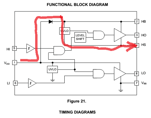
Could it be the case that HS pin negative transients due to parasitic inductances cause device overstress resulting in this symptom?


