This thread has been locked.

If you have a related question, please click the "Ask a related question" button in the top right corner. The newly created question will be automatically linked to this question.

TPS53319 layout example in datasheet

Other Parts Discussed in Thread: TPS53319

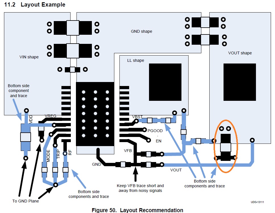
I would like to know about TPS53319 layout example on datasheet P.28.

There is a output capacitor between Vout shape and internal GND plane. What is this purpose? Is there any reason that this design has two kind of output capacitor which is connected to top layer GND and internal GND plane?

Best Regards,

Kohei Sasaki

  • I cannot see any special uuse for it. It appears to be just another output capacitor placed closer to the point of regulation where the VOUT trace is connected between the FB resistors and the VOUT copper pour.
  • John-san

    Thank you for your response.
    I found the following description on datasheet P.28 Layout Guidelines. Because there is description on the datasheet, I think there is any reason. Do you have any information?
    If there is no any special use, I will not care it.

    "Connect the ripple injection VOUT signal (VOUT side of the C1 capacitor in Figure 45) from the terminal of ceramic output capacitor."


    Best Regards,
    Kohei Sasaki


  • Sure, they are recommending that the VFB and ripple injection circuitry be tied to the output cap as I would also suggest. They could just as easily put all three output capacitors together at the top of the diagram and connected the VFB and ripple injection components there (as I would have done), but the original author of the datasheet did not do it that way. I suspect he did it just o make it easier to draw. I checked the EVM and all three output capacitors are located together (as I would design it, but I did not work on TPS53319 development).
  • John-san,

    Thank you for your reply. And I checked Application Report of DCAP device, it is "SLVA453". On this report P.5 and P.6, there is a description about ripple injection network layout.
    This report says ripple injection circuit should be placed close to the inductor, and I think this is different from datasheet. Should we follow in either?


    Best Regards,
    Kohei Sasaki

  • The ripple injection first R and C is directly in parallel with the inductor, so it is logical to place it adjacent to the inductor. In a well designed PCB, the output capacitors will be located close to the inductor as well, so it is not contradictory to have the Vout side ripple injection capacitor connected near the output capacitor positive side as well as close to the inductor.