This thread has been locked.

If you have a related question, please click the "Ask a related question" button in the top right corner. The newly created question will be automatically linked to this question.

TPS62133 power supply design (layout)

Other Parts Discussed in Thread: TPS62133, TPS62130, TPS2592BA, TPS25910

Hello TI and forum members! I am designing a 5V 3A power supply with the TPS62133. The most interesting charateristic of this regulator that attracted me was its high efficiency at low output currents (above around 81% @ 30mA and up to 86% @ 3A), which for higher output currents is not around the 94-96% other regulator achieve but more than doubles the maximum efficiency at very low currents when compared.

I have  several questions regarding the appropiate layout of the of some traces and components:

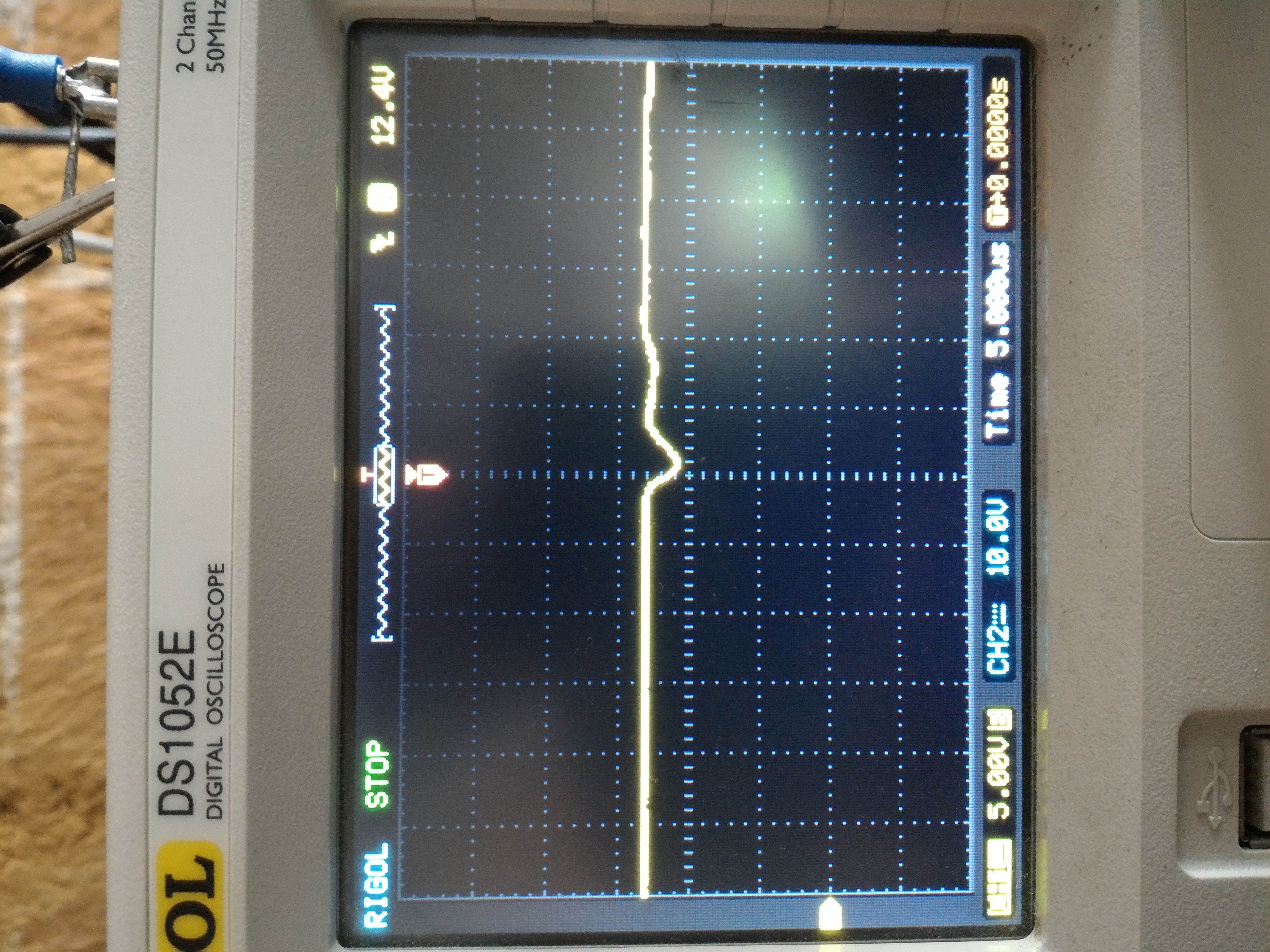
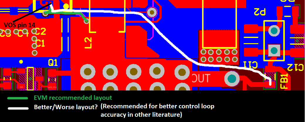
1. The VOS line in the EVM (SLVU437A) is routed from the VOS pin 14 through a via to the bottom layer, then through another via to the top layer and finally reaching VOUT just at the point where the output capacitors C3 and C4 are connected together with the inductor L2. This is not exactly the point where the load will be connected, which is the output connector J9 in the EVM. In my layout I have it routed in the same manner, not connecting the VOS pin to the point where the load will be connected but rather to exactly in the output capacitors (C2, C1) following what is stated in the datasheet and EVM. In other designs the pin that senses the voltage should be connected to the point where the load will be connected for the controller to be able to regulate the voltage at the point of interest. My question is: is the connection in the EVM good for all cases in this chip? Are there any assumptions made when making this connection at the output capacitors rather than the load?  Please refer to image VOS ping routing.png

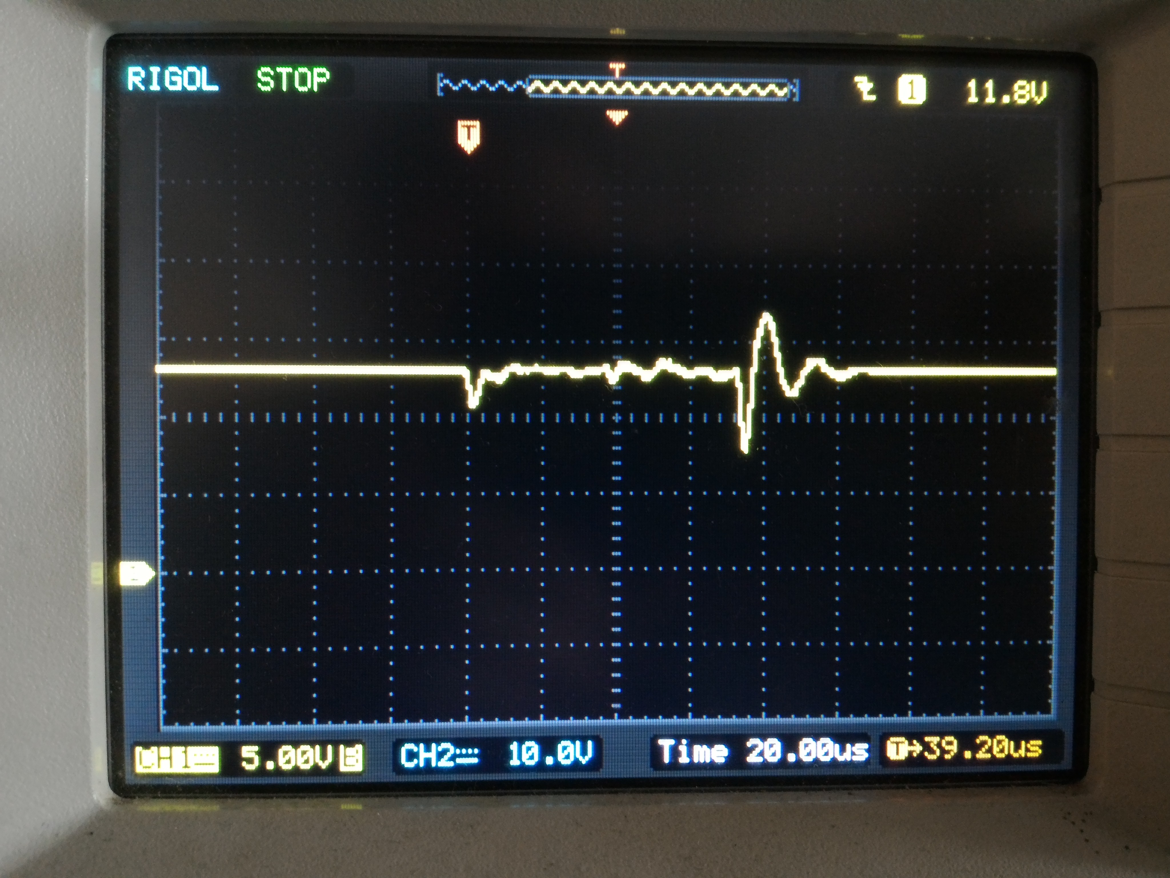
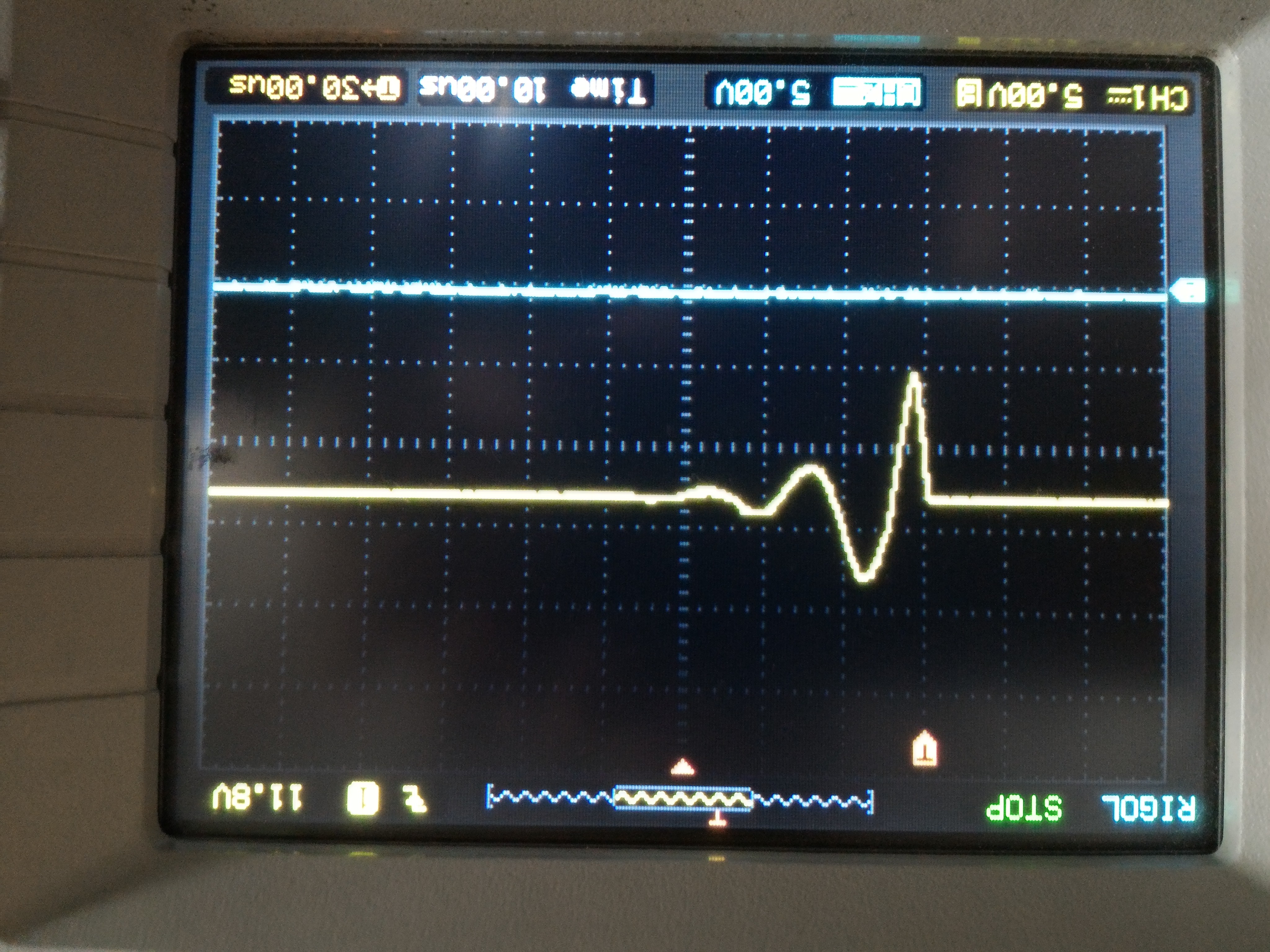
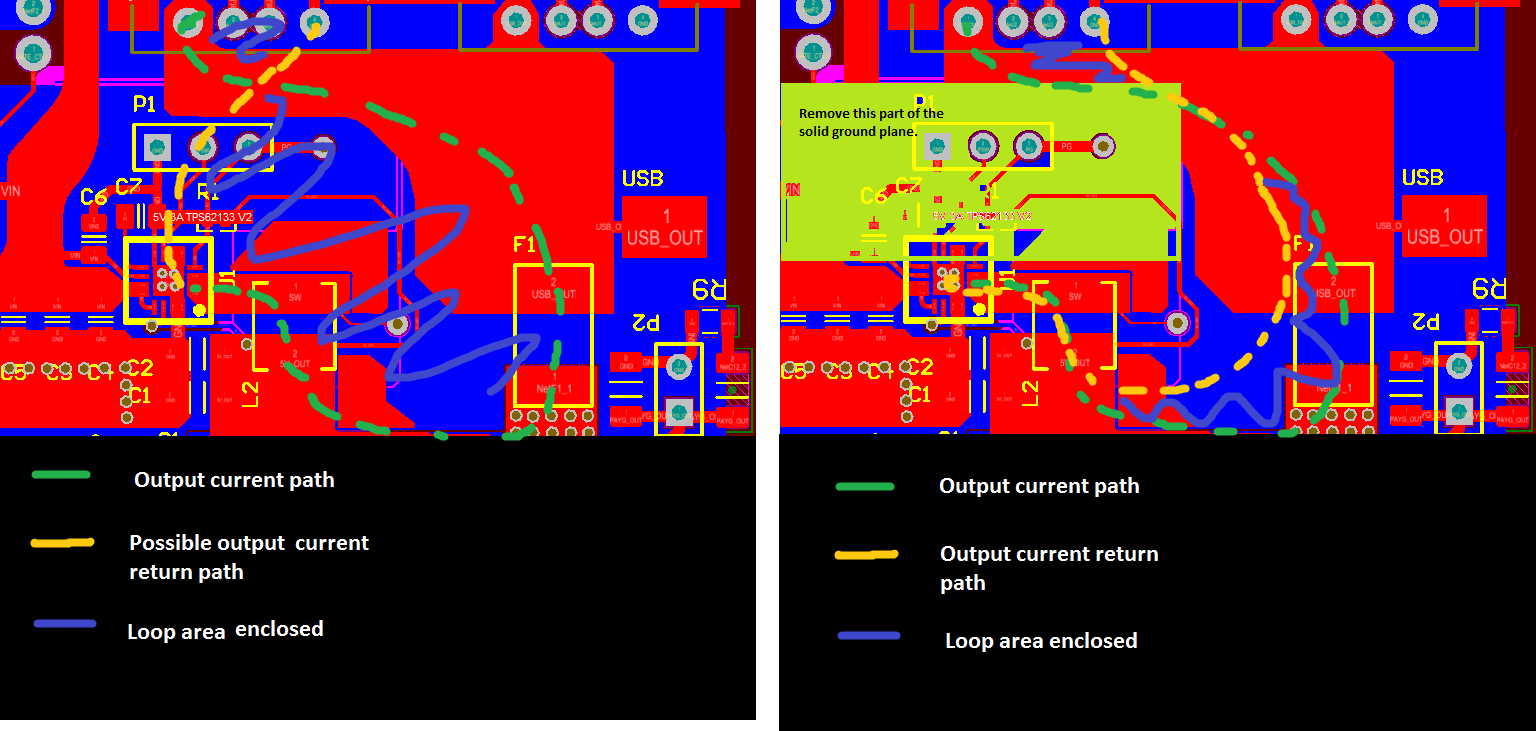
2. Loop Area for high frequency load currents: due to space/position restrictios in my application, the high frequency output load current needs to make a 90° turn near the IC.  Since the radiated energy is proportional to loop area formed by the load current (as is also stated in the TPS62133 datasheet SLVSAG7C) I am not completely sure a solid ground plane would be the best low impedance/EMI Absorbing path to be used, since it would enclose a relatively large area. Instead, I was considering to route this return path just above the output current path, so that the loop area is decreased to a minimum. Would this be a better approach?  or should the solid ground plane still stand despite the possible loop area?  Under the understand that high frequency signals will choose the lowest impedance return path, this path would be just below the output current path, in which case the solid ground plane would be unnecessary (at least for high frequency signals). The best decision is not clear for me, so is there any recommendation?  Please refer to image Return Path.png

I would greatly appreciate any feedback on this two inputs. The board was designed following as close as possible (and sometimes exactly) to the recommendations from datasheet and EVM, so I expect a first time working board within specifications.

  • Thanks for reading our reference documentation before doing your PCB layout. I would also note that you can order the EVM to get a PCB with no R&D effort on your part to experiment with your circuit.

    Yes, you should route VOS as shortly as possible to the output cap. It is not a remote sense input as in other devices. The FB pin is responsible for regulating the voltage setpoint.

    Your second question is not perfectly clear. I'll note that the inductor and output cap handle the AC currents in the output which is the critical loop to keep small. It should just be DC current going to your load which is much less dangerous to deal with.
  • Since for my application the position of the output connector is different from the EVM, should I allow the output current return path be through the solid ground plane or would it be better to route it only under the intender output current output direction in order to reduce the loop area?  

    By your comment on the inductor and capacitor, I would guess that the ground plane that connects the output and the regulator would serve only as return path for the DC current going to the load which is much less dangerous, as you said. So, that makes me think there is no reason for removing the ground plane to reduce loop area since anyways the current that would flow through that loop would be basically DC. Is this correct?  Thanks, sorry for not being clear from the beginning, I hope I am now! :)

  • Yes, ground planes are good to return DC currents. You should in general, have a ground plane.
  • Hi Chris, thanks for your feedback. I had several questions and points behind which I would like to treat:

    - You mentioned the VOS should be placed as close as possible to the VOUT voltage and the FB pin is in charge of the regulation. But in the TPS62133, which is a fixed 5V (TPS62133RGTR) the FB pin is grounded (as is recommended in the datasheet, page 3, pin functions). On the other hand, the VOS line is the "voltage sense in and connection for control loop circuitry.

    I understand and will follow your indication if you tell me that VOS line should be connected as close as possible to VOUT, you are the TI guy in the end and I am using an IC  you designed so I will stick to your indication, I just want to point out some reasons that did not logically lead to the answer you gave me, and in the end I am responsible for the product. 

    - Despite of the point above, I of course routed the VOS signal in my PCB as you told me and as all the documentation explains and show. The voltage regulation in the IC is really good at least in terms of noise at low (50mA) and high (2.5A) currents, with less than 30mV pk-pk voltage ripple across that wide range (I have not yet measured step response).

    - Regardind efficiency of the final design, I am at very good efficiencies  at high currents but not doing so well at low currents, which is a must in my application. In this sense, I want to ask you: Is there a private channel through which I can communicate with you? I would like to share some sensitive design files to have your feedback.

    Thansk for your feedback.

  • Yes, for the fixed output voltage versions, the VOS pin does both roles and must be connected close to the IC.

    See this app note for pointers on light load efficiency measurements: www.ti.com/.../slva236.pdf

    You should be able to start a conversation with me by 'connect' in the upper right corner.
  • To debug your efficiency, I recommend 3 items:

    1. Check the SW node frequency at higher loads to make sure you are operating at the lower setting.

    2. Measure the output current with a meter.

    3. Use the Coilcraft XFL4020 inductor to make your setup match the D/S. I don't believe your inductor's core material is ferrite, which generally means it will have higher AC losses which you would see at lighter loads.

    For a good thermal design, be sure and use thermal vias and make the GND area on top and bottom as large as possible. I don't think you will have issues with your maximum ambient, but that depends on how big your board is and how much other power is lost there.
  • Thanks for your recommendations. And once again sorry for my late reply.

    1.  I confirmed the switching frequency is 1.25MHz, i.e. the lower setting.

    2. Measuring the current with a meter did yield an increase in the efficiency, indicating the measurement was wrong. But the increase was marginal, of about 0.2%  for all output currents and input voltages.

    3. I will try to make the test to with the inductor. I actually tried to make this since the moment you replied but unluckily only samples of this  inductor are available to be shipped to my country and I have been waiting for them. 

    On another topic and an important issue to me, I have seen a somewhat strange failure mode of the device. When making some "stress tests" at high output currents (from 2A and up to 3A) the device fails after about 5 to 8 hours of continuous operation. I have made the test with 5 ICs and the 5 of them have failed in the same manner.  

    After the 3rd device failure, I was able to recover the device by reflowing the solder joints, but after repeating the test it failed again after 5-8 hours at 2.5A output current. The same happened with the 4th device, which failed in the same way, but was able to recover after reflow. One thing to note is that device No. 4, which was recovered, is able to stand more than 10hours at 2.5A output current after recovery. This is rather strange and might be indicative that the problem is not the IC itself, but maybe some other strange effect causing it to fail.

    After noticing this, I tried to do the same (reflow) with the 1st and 2nd devices but was not able to recover them. The 5th device also failed and was not able to recover it. 

    By failure I mean the following:

    VIN = 12.9V (Battery voltage)

    Input current = 7 - 10mA after failure, no output current (before failure Input current is around 170uA, no output current)

    Vo = 0.0V - 2.2V (open circuit output voltage), 0.0V when connecting any load.

    Io = 0mA

    SW node = 0V, no switching at all

    PG node = 0V

    So the failure is basically that the device cannot regulate again to 5V, which is a catastrophic failure. In all of the 5 cases the following characteristics were measured and confirmed:

    -Tambient = 24-26 °C

    -Max case temperature = 68°C

    - All other passive components of the TPS62133 were working OK because in each case I tested all of them with a new TPS62133 and it worked properly. (For every new test I used new components, to discard the probability of one passive component causing failure).

    I will of course appreciate your feedback about this failure mode and any suggestions about tests and measurements to make in order to determine and correct the root cause. Thanks a lot Chris!

  • By 'recover' do you mean that the same IC that stopped working, then worked again after reflowing it? This points to a possible issue in the first assembly of the IC. These are a little tricky to assemble with the thermal pad underneath.
  • Yes, the IC that stopped working, worked again after reflowing. This happened in 2 of 5 cases.

    Nonetheless, the 5 devices were working normally in the first try. If there would have been an assembly problem (of which I can only think about misalignment or bad soldering), then I think the devices would have not worked from the beginning, or if they had, maybe without proper functioning.

    On the other hand, it seems that the failure happens after some hours of sourcing a relatively high current, between 2A and 3A, given that they were able to operate for more than 24 hours at lower currents (1.5A).

    In any case, how do you think I can debug this issue with the IC? From the operating point of view, everything looks fine until that catastrophic failure happens.

    Are there any special assembly recommendations for this type of package? We have confirmed with our assembly house that they can, without any kind of problem, assemble this type of package (no issues with pin pitch, exposed pad, alignment, thermal vias underneath, position).

    Thanks for your reply.
  • That is very strange. A few ideas:

    You might see if there is a TI or distributor FAE local to you who could provide closer debugging.

    This app note discusses how to assemble this type of package: www.ti.com/.../slua271a.pdf

    You might take x-rays of a board which shows the issue to see if there is solder voiding under the part.

    Is the part/PCB very hot when this occurs?

    Have there been any changes to the schematic that you sent me earlier?

    Could you send a waveform of Vin, Vout, SW, and PG triggering on when the issue occurs (likely Vout dropping)?

    What do the markings on top of the IC say?

    Do you have a TI EVM with which to put a device which has failed onto to test?
  • Thanks for the feedback Chris. The appnote will be very useful when discussing assembly with our assembly house.

    1) As far as I know and Internet allows me to know, there is no FAE or distribuitor here in Guatemala. 

    3) About performing the x-rays, could you please provide more guidance. I have never done that to any PCB design.

    4) The part is around 68°C when the failure occurs, other components are at lower temperatures ( Inductor: 58 °C, Input/Output Capacitors: 40°C) and the copper planes around the PCB were around 41°C.

    5) There were no changes to the schematic. I should note that the 5th device that failed was tested in a new PCB layout that was basically the exact same as the previous one I sent you but with larger GND planes in top and bottom to allow for better heat dissipation, as we have previously discussed. Besides that, there were no other changes.

    Nonetheless, After some testing, it was determined that enabling the +5% Vout function through the DEF pin would be necessary. Also, I will add an input bulk capacitor of around 10uF 35V to improve input voltage ripple. BUT this changes will be made in the future final revision. In this sense, I would like to ask you:

        - Is it OK to connect the DEF pin to VOUT (+5V) through the 100kOhm resistor I am using to pull-up the PG pin? FSW pin is also connected to this node to set the lower switching frequency (for higher efficiency). Or is it better recommend to connect the DEF pin directly to VOUT? 

    6) I will try to get those waveforms. I hope leaving the scope trigger waiting for Vout drop works.

    7)The markings on top of the IC say:  QVZ , TI 48, A371

    8) I do not have a TI EVM to test the devices that failed, I will try to buy one and test like you mention.

  • Sorry Chris, I read a note in the datasheet indicating it is recommended to connect DEF pin to VOUT or PG. Please ignore my question about this.
  • Chris, I had another question for you. I forgot to mention :P

    In my application, the TPS62133 powers an internal circuit with an analog section which requires low voltage ripple. During our tests, we saw that adding a second 22uF X5R capacitor (exact same as the original "required" output capacitor) in parallel and just 1mm in separation to the original output capacitor, improved significantly the output voltage ripple (from 150mVpk-pk, to 100mVpk-pk) at low currents (7mA to 40mA), at an important output voltage in the analog section.

    Is it recommended to do this? I imagine it will have an impact in the control loop of the IC, probably to improve but I would like to confirm.

    According to the datasheet, the recommended configuration for "most applications" of the LC filter is 2.2uH, 22uF. I would be having basically 2.2uF, 44uF , and it is a combination recommended in Table 2, page 13 of the datasheet. So I imagine there will be no problems, rigth?

    Thanks!
  • Thanks for your responses.

    Given your constraints, it is likely not worth pursuing an x-ray. This would tell you if there was solder voiding under the part on the thermal pad.

    How was the temperature measured? To verify those temps, were you able to touch the PCB? Where you able to touch the inductor and IC for about 1 second only?

    Yes, connect DEF to Vout. Some customers would use the adjustable TPS62130 to give themselves the full flexibility of where to the output voltage.

    The test with the EVM would help to compare waveforms of a good IC (EVM IC) to your ICs. You could measure things like input current, SW node waveforms, etc. and then swap the ICs and measure them again.

    Yes, 2x 22uF Cout is perfectly fine. I would even recommend this much to overcome the 'DC bias' effect on the 5V output.
  • Yes, it might be hard over here to get a an appropriate x-rays, I guess we are not talking about using a "medical" x-ray machine.

    The temperature was measured using a K-type thermocouple and a PeakTech 2005 multimeter with +/- 1% accuracy. I was able to touch quite normally the IC and Inductor during high current operation for, say, some 2 seconds before feeling some heat transfer to my finger. Probably if I wanted I could touch it longer, but that was a good way to have a sense of how hot the IC and inductor were: not very very hot.

    Ok, I will connect DEF pin to VOUT then, not to PG.

    One question regarding the EVM. It would be this one, rigth? www.ti.com/.../tps62130evm-505. This one features the TPS62130, which is an adjustable version. I am using the TPS62133, the 5V fixed version to avoid external resistors, so probably I would not be able to test a good IC (EVM IC) because anyways I need to solder a TPS62133 which would be of the ones I bought.

    Thanks for your confirmation. Actually I used 10V capacitors to compensate for DC bias from the beginning, but this additional capacitor will improve capacitance performance.
  • Yes, that is the right EVM. There should be a section in manual on how to modify it to test out the fixed voltage version of the IC.
  • Hi Chris, 

    I would appreciate to have your input/suggestions about using the inductor NR5040T2R2N  instead of the XFL4020-222ME as switching inductor for the TPS62133. Please see the following links: 

    NRS8030T2R2NJGJ

    www.digikey.com/.../2666003

    http://ds.yuden.co.jp/TYCOMPAS/ut/detail.do?productNo=NRS8030T2R2NJGJ&dataUnit=M

    According to my calculations based on the recommended equations from the datasheet, it would be a fine replacement. But I would like to have your comments.

    The calculations are as following:


    Iout_max=3A

    Vout=5.25V (DEF pin high)

    Vin max = 14.6V

    L(min) = 2.2uH (ideal inductor)

    Fsw=1.25MHz

    Delta IL Max (peak-peak inductor current ripple) = 1.2A

    IL max (maximum inductor current) = 3.6A

    ILsat (minimum saturation current) = 4.32A

    NR5040T2R2N electrical characteristics and calculations:


    Inductance = 2.2uH +/- 30%

    Rated Current (max) = 4.8A 

    Isat(max,  30% inductance drop) = 4.6A

    Irms(40°C temperature rise) = 4.8A

    DCR = 15mOhm (typical), 19.5mOhm (max)

    --Minimum requirements based in this inductor's characteristics:

    Minimum Irms required @ Isat inductance drop = 4.62

    IL_max required @ Isat inductance drop = 3.85A

    Since    

                  Irms (40°C temperature rise) > Minimum Irms required @ Isat inductance drop

    and

                 Isat (max, 30% inductance drop) > IL_max required @ Isat inductance drop

    and the DCR is relatively low, I think it would be a good option.

    What do you think?

    Thanks for your feedback.


  • Yes, it looks fine.
  • Hi again Chris,

    I hope you are doing great.

    I have been looking for options to protect the output of the TPS62133. I am interested in integrated solutions, and came to know the eFuse product range from TI. From all the options I have selected the TPS2592BA, which works for 5.25V and programmable current limit.

    The TPS62133 datasheet SLVSAG7C, does not specificy accurately its short circuit protection performance, nor gives graphs about response time or tests. Do you have any opinion regarding this selection of protection device? Would you recommend any other?

    Also, since the TPS62133 does not have reverse polarity protection, I have selected the SS3P6 Schottky Diode for reverse polarity protection (vishay.com/docs/88997/ss3p5.pdf). This diode is designed for an average forwared current of 3A at (120°C max case temp). It will handle no more than 1.4A average forward current and a corresponding 0.5V drop, for around 0.7W loss on it, which is exactly good.

    Do you have any suggestions/opinion on this topic?

    Thanks again for your feedback.
  • Yes, you probably need some sort of fault protection on the output if you're powering a USB port or other 'user-accessible' terminal. These devices are supported in the power interface forum.

    The TPS62133 does specify its nominal current limit. We give a typical value for the reduced current limit during a short. This is cycle by cycle protection, so it will keep the current below the specified level at all times.

    Do you need reverse polarity on the input or output? A diode in series with Vin is the easiest way to get reverse polarity protection on the input. See also this app note: www.ti.com/.../slva139.pdf
  • Thanks for your reply Chris.

    I have asked some questions in the appropriate forum, but so far I have got no answer. So thanks for your reply. 

     I will consider the options of using a mosfet instead of the diode...very price dependent.

    Thanks,

  • Hi Chris,

    This is Juan again. I hope you are doing great. 

    Related to my previous post on output protection for the TPS62133, I have choosen the TPS2592BA. The system I am designing has another 12V, 5A output connected to the same 12V, 12Ah SLA AGM battery which supplies the TPS62133. This other output has also an output protection device, the TPS25910. 

    When making some tests on this last device in the actual system, making a hard short circuit on the 12V output (Output ON, then short circuit) I have measured that the voltage input, which is the battery, swings due to the high short circuit current. This produces a swing in the input voltage of about 15V, which makes the input voltage reach approximately 20V. This voltage will be present to the input of the TPS62133, and, since is beyond the recommended maximum input voltage (17V) and just exactly at the Absolute Maximum Input Voltage (20V) it has raised concerns. Beyond that, during one short circuit test, I was able to damage one of the TPS62133.

    I am thinking about using a TVS to suppres those voltage spikes that can be generated during a short circuit event, or any other event that can produce suck spikes in the input voltage. The question is, what would be the recommended maximum clamping voltage for the TVS to protect the TPS62133? Should it be under 17V or 20V?

    If I had no other constraints I would obviously use one with Vclamp<=17V, but the issue is the following. Since the battery needs to be recharged constantly, the maximum voltage it reaches during recharge is 14.7V. So the TVS must have a reverse working voltage >14.7V. Normaly the TVS diodes clamping voltage is around 40-60% above the reverse working voltage, so I have found options that either: have a reverse working voltage over 14.7V but a clampling voltage well over 17V (19-26V) or have a clamping voltage below 17V, but a useless reverse working voltage (11V - 14V), taking into account not only nominal specifications, but minimum and maximums.

    Choosing a TVS with a maximum clamping voltage below 20V might aliviate this situation, but I would be outside the recommended operating conditions. 

    What do you recommend to do? Would it be OK to use a TVS with a  17V<Vclamp<20V?  I am attaching the waveform of the battery voltage. You can see there the duration of the event is in the order of 5-7us. Would this immediately/slowly damage the TPS62133?

    Thanks again for your support.

    The Blue Waveform is the input voltage from the battery during the shorcircuit event, you can see that its around 13V before and after the short. The green waveform is the current during the short circuit at the other 12V output (it reaches almost 60A). I will send via private message the updated schematic for clarity.

  • Yes, you can clamp above 17V for your situation. I would ask you to measure the Vin right at the IC's pins with a scope to see the real waveform.

    More input capacitance is another possible solution. As well, a series element like a small resistor or small inductor might help separate the two nodes. We also have this reference design: http://www.ti.com/tool/PMP9757
  • Thanks for your response. I am attaching some pictures of the waveform right at the IC's pins. 

    Adding more capacitance did have some marginal impact, reducing the voltage spike around 500mV on averega, but that is not enough. Thanks for the reference to the appnote. I already went through it, but I need to analyze it more in depth.

    I have one more question regarding this device. The TPS62133 is also the supply of a 5V MCU. Due to this, when the MCU needs to be programmed in circuit, there is an external 5V power supply from the programmer that supplies the MCU during programming. During programming the TPS62133 has no input and thus is off. Nonetheless, the external 5V will appear in the SW, VOS and PG pins. Do you see any problem with that?

    Thanks

  • Yes, it is usually ok to bias the output like this. Note that if Vin is not present, then the voltage on the output will appear on the input through the high side MOSFET's body diode.
  • Understood Chris, Thanks for the information and clarification.

  • Hi Chris,

    Hope you are doing great.

    What is the best way to left the PG pin on the TPS62133 if will not be used?  Should I leave it not connected or connected to GND. Since it is open-drain, and activates when Vout regulates, I guess leaving it unconnected is OK. I imagine I could connect it to GND so that it never is at high impedance.

    Thanks for your feedback.

    Juan

  • Yes, either floating or grounded is ok.
  • Ok, thank you very much. Will leave it floating.