This thread has been locked.

If you have a related question, please click the "Ask a related question" button in the top right corner. The newly created question will be automatically linked to this question.

TPS54560 - custom board cannot maintain high amerage and makes a loud sound

Other Parts Discussed in Thread: TPS54560, TPS54550

Hello,

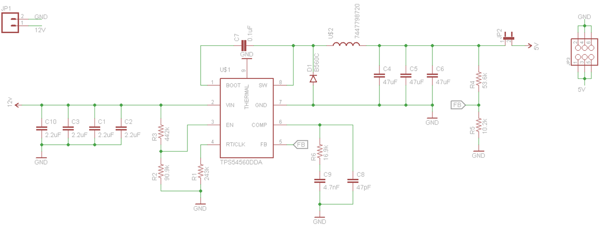
I designed a custom board with TPS54560 following the design example from the datasheet ( www.farnell.com/datasheets/1857574.pdf  page 24). It's supposed to convert 12v to 5v.

So it works when I power a small LED, but when I plug some higher load, such as an LCD, the board starts making a strange sound and seems to kind of "reset" - can't maintain its high current.

I'd be very grateful if you can give me any hints on what I may have messed up, since I'm very noob in PCB design.

The sound is some high frequency "hiss", like white noise from an old tv, I think it may be coming from the inductor, but not sure. Even more this sound makes into my audio speakers somehow. I use a computer PSU to generate the 12V for the board, I guess from there it goes back to the mains plug, then into my PC - youtube - and out from the speakers :)

But when I power a small LED, instead of the high load LCD - no such sound happens.

I tried powering a dev board also, which takes 5v/2-3A - same thing. Just the LCD itself draws about 1A current, board ~2A - both together - ~3A I measure that using an onboard jumper.

So it starts, after ~1-2 seconds it kind of "resets" - power goes down and starts again. This is seen both on the ampermeter and heard from the sound. Also the LCD/board cannot properly power up.

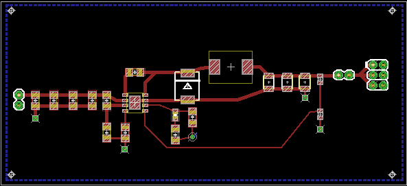
Here are my schematics and board design. Schematic is the same as in the datasheet, just a current-measuring jumper added:

The inductor and diode are the ones suggested in the datasheet.

A few notes:

- I couldn't find the exact resistor and capacitor values for all of them, so sometimes I used approximate values to those shown on schematic. This results in ~5.25V output

- the thermal pad on TPS54550 is not soldered, just touching it - is this a problem?

- first I tried with a homemade PCB, then I got a proper PCB from a fab house - same thing

- I'm not sure how wide/thick the traces should be, so now they are pretty much random. I made the main power traces wider though - they now match the width of the TPS54560 pads. 

Can you give me any hints on what I may have messed up?

Thanks!

  • I'm getting someone to look at this. I can tell you up front that you will have issues with that pcb layout. My colleague will follow up shortly.
  • Hi Lacho,

     John just told me that you have some issue in PCB layout for TPS54560. I checked your SCH, it is the same to reference design, so I think it is ok to use the approximate value, even though they are not absolutely the same.

    Actually, there is a layout guidelines in the datasheet(page 37), you can take it as a reference. I'm sure it will be helpful. Here I want to highlight some tips:

    1. Identify which path is dirty(so many noise), and which is clean, also, which signal is sensitive and which is robust.

    a. For a Buck power path,the switching loop of Cin, HS FET & diode will be dirty, and the loop of inductor & Cout  will be a litter better as the current is continuous.So try best to keep the dirty loop smallest, and it will reduce the system noise. You also need to keep the inductor close to the SW/PH pin.

    b. For a controller, FB & COMP will always be the sensitive signal. Try to make them far away from the high current power loop.

        RT is controlling the system frequency, you also need to keep the RT close to the RT pin and a clean GND.

    2. Grounding

    a. If there is powerpad, try to have a strong connection to ground, it will very helpful for reducing noise and improving thermal performance.

    b. If you have enough space on the bottom layer, make sure to have a big whole piece of GND fill on it.

    c. Try to keep all the sensitive signal ground together, and then connect to the GND pin or powerpad(Single-point ground).

    3. wide/thick

    Try to use 2 Oz and much wide for power path.


    Kim Yang

    SWIFT

  • Hi Kim,

    thanks for the reply, I'll redesign the board with your suggestions.

    Edit: I now checked the layout guidelines in the datasheet - I had totally missed that... Indeed the suggested layout is very different from what I have, hopefully that should fix it.


    Regards,
    Lacho

  • Hi Lacho,

    If this issue fixed, please kindly share the experience here, so that others can find it as a good reference.

    Kim Yang
    SWIFT
  • Yes sure, I'll redesign the board but the fabrication process will take about a week. When it's ready I'll post the results.

    Cheers,
    Lacho

  • You might want to post some screen shots before you send the files off to the board shop. We can check your layout first.
  • Oh thanks a lot, that would be very helpful.
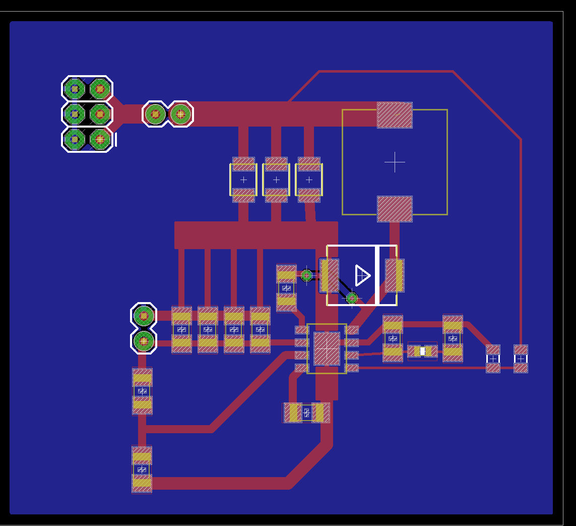
  • Ok, so here is what I got:

    I tried to stick to the suggested design as much as I can, but not sure if I managed very well...

    The input and output capacitors in my case are 4 and 3, rather than 1/1.

    Also I couldn't place the 6 vias under the IC... for some reason the smallest via that Eagle allowed me to do was much larger to fit six in there. So the ground connection is now done from the input power pin. If this is too bad I may try to manually drill some vias when the board is ready.

    And I may try to do a homemade version of this, there's only 1 connection in the bottom layer, I'll see if I have any luck.

    Will keep you posted.

    Cheers,

    Lacho

  • So I did a quick homemade board from the above, soldered it, but I now get ~2.3V output :)

    I started debugging it and see that the output voltage divider is showing weird resistor values... on the schematic that I posted this is R4 and in my case it's 56k (since I couldn't find 53.6k value). When I measure it while soldered, this shows ~22k. If I measure it backwards - it shows ~15k. I suppose the diode may have something to do with that difference...

    And when I calculate it using the output voltage equation from datasheet (section 8.3.6) - it seems right - when that resistor is ~22k the output would be ~2.3V. So I suppose this resistance is the problem (I may be wrong though, I'm really not an expert).

    If I unsolder either the diode or the inductor - the resistance becomes right - 56k. I tried powering the board without the diode - it gives the expected ~5.2V, but looks like it cannot supply high current.

    I triple-checked the board for shorts and other weird things - so far everything seems fine to me. I'll keep digging, in the meantime if you notice anything wrong in my design, please let me know.

    Regards,

    Lacho

  • Take a look at the layout in this document:

    For 5 A lad the TPS54560 will dissipate quite a bit of heat.  The vias under the thermal pad are essential.  You should be able to specify the via diameter, I think we use 10 mil, I would have to double check next week.  Also note there are two internal layers dedicated to thermal dissipation ground.  Pay close attention to the shaping and connections of the input and output voltage copper fill areas on the top and bottom sides.

    And yes you cannot measure external component values in circuit as you have observed.

  • Right, I managed to create the thermal vias, it was a silly mistake. I didn't know there was an EV board, that would be very useful, I'll use it as a reference.

    Thanks a lot!