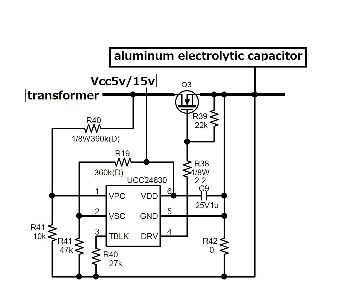
This thread has been locked.

If you have a related question, please click the "Ask a related question" button in the top right corner. The newly created question will be automatically linked to this question.

UCC24630 / the high current on primary-side FET.

Guru 11170 points
Other Parts Discussed in Thread: UCC24630

Hi all,

Would you mind if we ask about the high current on primary-side FET on synchronous rectification using UCC24630?

<Our recognition>

When the operation of the power supply switches from CDM operation to CCM, the high current flows the primary side FET.

We guess that turn-off delays at the secondary side FET caused it.

In this moment, due to turn-off delays at the secondary side, the primary FET and the secondary FET switch ON at the same time.

So, is our recognition correct?


  • Hi Yoshitaka, 

    I'm not sure if there is an image missing from your post. Can you post your schematic and the waveforms on the primary and secondary drain (switch) nodes during the cross conduction interval. With the UCC28640 it is important to size the resistors on Pin 1 and Pin 2 correctly to ensure no cross conduction. 

    Thanks

    Billy 

  • Hi Billy,
    Thank you for your response.
    The high current occurs irregularly.
    Reproduction is difficult.
    The figure of waveform did not get out.
    We are aware that it occurs when the operation was changed from CDM to CCM.

    We guess that it is the cause of secondary side FET.

    Could you let us know why the high current flows primary-side EFT?

  • Without a schematic or some waveforms it is difficult to say. It may be caused by incorrect resistor values being connected to pins 1 and 2 of the UCC24630 as I said.

    Note that in CCM, if the switching period can change by more than 600ns in one cycle, e.g. due to frequency dithering or variable frequency operation, the UCC24630 is not compatible with the operation of the cirucit.

    This is explained in section 8.3.3 of the datasheet.

  • Billy-san


    My customer showed a schematic around UCC24630.

    I will attach it.

    Could you understand the cause of the failure in this schematic?

  • Without the input voltage range and turns ratio, I'm not sure what the value of R40 should be, but the ratios seem reasonable so I expect that the issue is that the primary side on time is increasing by more than 600ns in one cycle which is causing cross conduction.

    Thanks

    Billy

  • Billy-san

    I'm sorry to ask you many times.

    This power solution type is Fly-back structure.
    The transformer turns ratio is 65 : 3.
    Minimum Vin=90Vac.

    We heard from our customer that the primary side FET has broken when a high current flows into it at Vin = 90Vac.

    We recognize that it is not enough information to , but if you have any idea to identify the cause of it, could you let us know?

    Best Regards.
    Nagai

  • Hey Nagai,

    See page 17 of the datasheet, section 8.3.2.

    If the reflected ring voltage exceeds 85% of the minimum bulk voltage for > Tvpc_blk, the controller interprets this as a primary on time, and at the end of this misinterprted 'on-time' it gates on the SR. This can cause shoot-through if the main FET turns on again at the same time.

    With the turns ratio in the design, assuming the minimum bulk voltage @ 90Vac is ~ 80Vdc, and assuming from the schematic that the design is 5V out (and not 15Vout), this gives a reflected voltage of 107.5V, which is well above the assumed 80V minimum.

    I recommend changing the transformer turns ratio so that the reflected votlage is < or = the bulk capactior minimum DC voltage, probably 70-80Vdc @ 90Vac as mentioned.

    Hope this helps.

    Thanks, Billy

  • Billy-sanYour answer was very helpful to me.Thank you very much.Nagai.