Many times a power design will have multiple inputs.
Diode ORing is the term used to allow automatic selection of the input source.

Usually the diode that is shown is just a representation of what is done in practice.
Diodes have loss due to their forward voltage, Ploss=Vf x Iout
Unless the diode has some means of control, the highest voltage will dominate and be passed to the output.
If you want to control which input will supply power, the diode must be controllable.
Suppose PS1 is desired to be used if present, use PS2 only when PS1 is not there.
And suppose PS2 has a higher voltage than PS1.
: IF PS1 is present THEN use it, ELSE use PS2 IF present.
IF THEN ELSE, software terms.
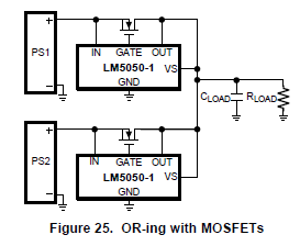
Mosfets can be used, but remember they have a BODY DIODE, so even if you used an ORing controller you still have the diode function.
LM5050-1 is one such example.
Even if you turn off the N channel FETs, their body diode will conduct left to right.
So again the highest input voltage will dominate.
To solve this, you can put 2 FETS back to back.
Here is an example of the TPS2490 family with Reverse Blocking.
Q1 Q2 the body diodes point away from each other. The FETs are controlled together.
So when both fets are off no current can flow either way.

Thus you can prevent the higher input from dominating a Diode ORing design.
The lower voltage input could be selected if desired.
Back to Back FETs are also useful to prevent backfeed from a reverse current from from an output to an input.
This method can be adapted to many ORing and Hot Swap controllers.
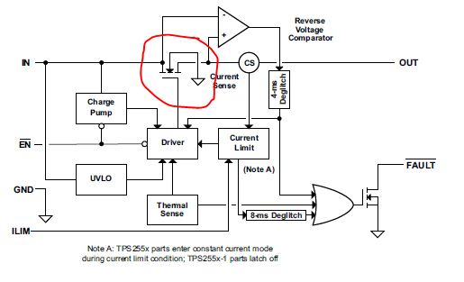
Another way to block reverse current is to remove the body diode of an internal mosfet switch.
TPS2552 is an example.
The block diagram of the device shows the center gate lead of the internal FET tied to ground.
This can be done during the IC design, however not done with discrete mosfets.
Seeing this method in the IC block diagram will let you know that the body diode has been effectively removed.
There will be no reverse conduction.
A lower voltage input may be selected in an ORing scheme.