This thread has been locked.

If you have a related question, please click the "Ask a related question" button in the top right corner. The newly created question will be automatically linked to this question.

BQ24133

Other Parts Discussed in Thread: TPS63020, BQ24133, BQ24630

I am debugging prototype BQ24133/TPS63020  battery support design for single cell application.

It uses a BQ24133 driving a TPS63020 buck/boost to keep output voltage constant at 5V over tolerances  in adapter and battery voltage.

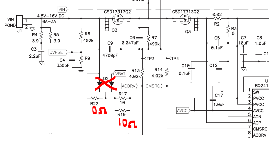
Critical parts are  the same as EVM PCBs, modified for my application  and  which operate as expected.


However, when operating my combined  board design  with an adapter to support a load and battery charging, I’m encountering an issue ..

It appears that that when the load current approaches about twice  the design charge current, the charge current starts pulsing.

Also there appears to be no dynamic current management. When charge + load  current exceeds ACset values the charge current pulses (not decreases)


If allowed to continue the charging terminates and the LED current blinks, I assume, as a charge termination condition

This becomes more sensitive as the battery voltage approaches its full charge, and the charging never enters a constant voltage/ charge taper cycle.


I‘ve tried many things to tickle  this issue , some of which include.


1)      Add/change caps and resistors shown in the EVM

2)      Set OVPset to 1 volt.

3)      Reduce charge current

4)      Use DC load resistor, and clean power supply to eliminate any noise.


Can anyone  give me more  ideas to explore so I can  understand  what’s going on?

  • Hi James,

    Can you please share a schematic so I can better assist you?

    Thanks,
    Rachel
  • How do I send you a schematic?.
    I don;t see an obvious way to do this?
  • If you have Altium, I can send you the entire project....Thanks.....................Jim
  • James,

    If you can generate a pdf file from Altium and then you can attached it.  At the lower right of the textbox you write posts in there is a "use rich text formatting" option which will give you more options to attach a file.  I think the regular post window might also support drag and drop for attachments. 

    Please let me know if you need further assistance.

    Thanks,

    Rachel 

  • James,

    Overall the schematic looks pretty good, but can you tell me what the purpose of Q1 is intended to be?  I also recommend making your OVPSET level a little more tolerant.  For a 5V input, a 7V OVP would be typical. 

    For clarification, the STAT pin is only blinking after some time in this pulsing condition, but not immediately blinking, and not blinking for Adapter only or Battery only conditions? STAT blinking is the FAULT indicator for this device so it's a good thing to start with. 

    Can you check the ACDRV and /BATDRV signals match the datasheet capture one the condition of adapter plug in? Are they steady state after the adapter is plugged in?

    Can you measure the current across the sense resistors (R6 and R7) and calculate the current and see if they match the set points.  This would help indicate if there is some bad current path in the layout that we're not seeing. 

    Thanks,

    Rachel 

  • After a week of looking at this, it turns out the EVM board is populated  to connect  the adapter input  (VIN) directly  to AVCC and bypass the "oring" diode D2 shown in the EVM schematic. (ref R22 in the EVM schematic)

      It appeared that as my adapter input got close to Vbat +.9V  the device began to oscillate between adapter input and battery input and  the charge circuit  went discontinuous as observed with the pulsing..

    I also did not use schottky diodes (low drop) to "or" Vbat and VIN on my PCB , so my adapter input had to stay at least .7V to .9V above  Vbat  in order to behave reasonably.  For a fully charged battery this would around 4.9V

    After shorting Vin to AVCC in my design, the circuit behavior greatly  improved, eliminating any pulsing or erratic adapter/battery switching. I left the diode that "or's"  Vbat to AVCC when VIN goes away. The adapter input can now go down to 4.5V without erratic behavior, and will probably improve if I use as schottky  diode to "or"  Vbat to AVCC. I have to explore the circuit behavior using a a dual schottky diode to "or" both, VIN and Vbat to AVCC, rather than shorting VIN to AVCC.

    ACDRV and BATDRV make their full on and off swings as expected, ACDRV swings up to CMSRC+6V to drive the N-channel gates. 

    Measuring the SRN/SRP, and ACN/ ACP is difficult without special differential equip. which. I don't have.The DPO 7254 scope I have can do some with special probe treatment,  but can't discern 5mv signals in an environment which has 50mv of common mode noise. Even the EVM boards appeared this noisey. However, once VIN=AVCC the battery charge current level ,taper cycle, and dynamic power switching appeared to operate.

    The BQ24133 pin out is not very friendly to getting short traces on both SRN/SRP and ACN/ACP, one set has to be long if a P-FET is going to be used to switch the battery to Vsys. The EVM board made SRN/SRP traces long but believe used a shielded inductor to mitigate this. I will change the inductor and see if traces  can be made shorter and more isolated from circulating charge circuit buck currents. I am very concerned about this and have used techniques suggested by   power  design consultants in the past to determine optimum layer stack-up and routing, but I am also limited by real estate connector  placement requirements.

    Things look much better  this once Vin is directly connect to AVCC,  and I  must further investigate your suggestions.

    From previous exposure,  I see that back-back p-channels used as the adapter input switch in  BQ24630 designs already provide the dual diode "oring'  function  to AVCC via P-FET drain body diodes.  Dual N-channel drain body diodes face the wrong direction forcing an external  dual diode to provide the function.

    Thanks Jim

  • OOPs...... Q1 is used to switch a status line and indicate when Vout is being operated from battery only.
  • James,

    So it sounds like you found your issue is that your 5V input minus the diode drop was hitting the sleep comparator and causing the IC to change power path selection from input to battery which was created the "pulsing" condition.  Is there anything else I can help you with?

    If the circuit is otherwise working correctly there is not need to measure across the sense resistor, I was just using this as a troubleshooting process.  All that is needed to measure this is a voltmeter across the resistor and the measured voltage drop can be used to calculate the current using the sense resistor value.

    If you reference the bq24133 EVM, you can see that there is a 5V version (-001) and the BOM will show the differences in population from the full voltage version, primarily as you have found they omit the dual OR diode to ensure that AVCC has enough margin over a nearly fully charged battery to continue proper operation.

    Regarding the SRN-SRP trace lengths, the EVM layout is a good general purpose reference, do you have a specific concern I can address?

    For detecting adapter vs battery power, we typically recommend using REGN because it offers a tested load capability.  The /BATFET driver isn't designed to support additional circuitry.  I have seen cases of using /BATFET work just fine, but it's possible to overload it.

    Some additional feedback on your circuit:

    • C7 and C1 should be changed to uninstall
    • Because of the switching nature of this device, if you product has specific EMI performance requirements please ensure your layout follow best practices to minimize emissions.  You can also add the following to allow for tuning of the SW node after production to improve EMI performance:
      • Add 0-ohm resistor on BTST in series with C4
      • Add an RC snubber from SW to PGND, this can be left as uninstall unless needed
    • C5 should be 1uF
    • I think there are some other changes from the EVM schematic, you might want to double check.  I just wanted to make sure you're aware and that they are a specific design choice, not mistaken ommissions. 

    Please let me know if there is anything else I can help you with.

    Best Regards,

    Rachel 

  • Problem in my single cell application now is when VIN is shorted to AVCC to prevent the sleep timer from kicking in at low tolerance adapter voltages the battery is loaded by the the adapter source impedance when if it is not entirely disconnected. Looks like the input snubber may also be advisable if AVCC sees the raw adapter input.
  • James,

    Can you explain "the battery is loaded by the adapter source impedance when if it is not entirely disconnected" I'm not sure I'm following.   VBAT should have no direct connection to the adapter voltage.

    The EVM and the datasheet provide additional details regarding recommended input conditioning which should help, please check section 10.2.2.4 Input Filter Design.

    Thanks,

    Rachel 

  • Ref EVM schematic, figure 8  SLUU476

    Unless I'm missing something, the only way I see to have AVCC supported during battery only operation is to "or"  VBAT into AVCC   via  the  D2 diode  shown in the schematic .

    If  R22 also  shunts  VIN to AVCC  to keep the sleep timer from kicking in.  then the adapter input  will be  driven by VBAT thru D2 during battery only operation  adding extra load to the battery. This is 65ma for my adapter.

    To fix this I'm using a schottky dual diode (BAT54C) to "or" both VIN and VBAT to AVCC. The Vd is only 200mv.

    When the dual diode is used to "or"  Vbat and Vin  to AVCC, then... when the battery only operation occurs, the diode in series with Vin will block Vbat from driving the adapter input.

    My problem is when the adapter is providing Vin and the battery is at full charge (~4.2V) 

    My adapter input is 4.9V minimum so in this case AVCC will be 4,7V 

    Since AVCC has to be at least 4.5V (specified)  to charge the battery (and assume keep the sleep timer from going off)  this will work with a 200mv margin.

    My initial design used a BA70 dual diode which had a .7V to .9v drop, forcing AVCC below 4.5V when the adapter was at 4.9V.

    Close but it seems to work in my prototype.

    Hope I'm  making sense.....Thanks .............Jim

  • James,

    I think the confusion is that we use the same EVM for both 5V and 15V options.  If you look at the BOM page you can see that for version -001 the diode OR is omitted.  VIN is connected to AVCC but VBAT is not, additionally there are changes to the biasing of the BATFET gate.  

    Best,

    Rachel

  • Rachael,

    Thanks for your patience. So I did miss something.

    To confirm whats going on with the EVM......when Vin shuts down, topside of R8 is powered by Vsys via drain body diode of Q4, but  R10 pulls down, turns on Q4 Batfet , and the BQ24133  goes  unpowered?

    Thanks...............Jim

  • Jim, 

    You're correct. Q4 is passively turned on and the bq24133 goes unpowered in the 5V configuration.

    Thanks,

    Rachel

  • Now that I understand whats going on I 've made design corrections and will be getting new prototypes.3731.97-13424LC1 - Schematic.pdf

  • Rachael,

    Just wanted to let you know I got prototypes back. I actually finished the project a few weeks ago.

    To review, I was using the BQ24133 to manage and single cell battery and power adapter to drive a TPS63020 Buck Boost Controller that maintained  a 5V output for a processor control board.

    Layout was a challenge to keep the single point grounds at the power pads and circulating switching currents over the top of each each in a cascading power converter design. I did this in a 4-layer design. The BQ24133  both charges the battery and sources current from the adapter or battery which added complexity.

    Everything operates as expected. Battery and adapter transition is seamless from about 3.5V (battery) up to 5.5V( adapter) @2.5 amps. Noise and EMC look low but haven't actually done formal radiated measurements yet.

    This design structure will be used in other products we make.

    Your help was invaluable.....Thank you.......Jim