This thread has been locked.

If you have a related question, please click the "Ask a related question" button in the top right corner. The newly created question will be automatically linked to this question.

LM5576 EMI Isuues

Other Parts Discussed in Thread: LM5576

Hi,  I am using LM5576 to convert 24V to 5V. I see that EMI performance is not good with 24V input. It is significantly better with a 12V input. I am using power adapters with CE mark for both 24V and 12V input. I want to use 24V only as input.The maximum load current is about 250mA. I am suspecting that since the load current is too small for this kind of regulator, these kind of issues are coming out. Did anyone face this kind of issue? Any help to improve the EMI performance will be appreciated.


  • Hello Sahitya, 

    With this load current the regulator is probably operating at much lower frequency at 24Vin than 12Vin, since the part is probably in discontinuous mode of operation. Since the frequency is shifting, the EMI profile will change as well. 

    How do you determine that the EMI is worse? Are you running a radiated EMI test or conducted EMI?

    You can post your schematic and board layout here and we will be happy to review and recommend some improvements. 

    Regards, 
    Denislav

  • Hello Denislav,

    Thank you for a reply.

    Yes, we ran a Radiated EMI test on our board and observed these issues.

    Below is the schematics for the regulator.

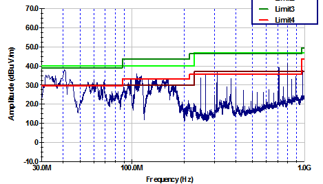
    I am also posting the RE results for your reference. We are concentrating specifically on Cisper Class B.

    24V

    For 12V supply the noise floor is down by approx 10dB.

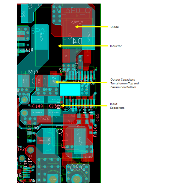
    The Board Layout is as shown below.

    Please review them and let me know what you think.

    Thank you.

    Sahitya

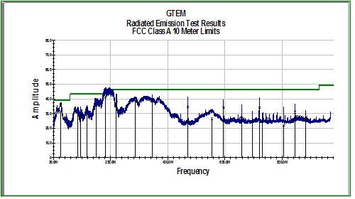
  • What a coincidence... I'm sitting in an FCC testing lab seeing a very similar radiated EMI issue up to 430Mhz, with a particularly noisy area between 200-250Mhz.  I have isolated all other parts of the board, and the LM5576 is the only thing running now.  I am using 48V input and I get:

    Schematic:

    I can't speak for Sahitya, but my project is rather urgent.  Anything you can do to provide a timely response to these issues would be greatly appreciated!

    Thanks,

    John

  • Hi John,

    Since you are sitting in the FCC lab and trying for your board to pass, I would like to give you quick suggestion. You can use a Snubber RC Circuit across the diode D11 and try. We tried that and got better results. :)

    Thanks,

    Sahitya

  • Hi John and Sahitya, 

    The snubber is a good idea. It adds some losses, but if you have to use it, it is available. Another "tool" would be to introduce a resistor in series with the bootstrap capacitor (BST pin). This introduces resistance in series with the high side MOSFET gate drive and essentially slows down the switch transition edge rate. Resistances in 1-10 ohms are a good starting point. Similar to the snubber, this also adds efficiency tradeoff, but it is way to bring noise/ringing down. In this case the power is dissipated in the IC, as opposed to the snubber. If you are already operating in high ambient temperature, may be the snubber is a better choice because the heat will be spread in another component instead of the IC.

    Sahitya,

    I looked at your layout. I like the input capacitor position. One improvement would be to connect the CIN ground copper directly to the large IC GND pad (instead of going through vias). Vias in the switching current path add inductance which converts to voltage spikes. The input capacitor GND connection in a Buck converter to the low side switch (the PGND pin of the IC) is a high di/dt. Any inductance (think current loop area, traces, and vias) together with the high di/dt will convert to noise.

    Here is a way to improve the connection:

    I see that the catch diode is on the opposite side also, sending the high dv/dt SW node to another layer. This is also not ideal, but you probably have some board area limitations if you are doing it.

    Do you also need to pass conducted EMI? Most of the noise on the Buck converter is on the input side.  Placing additional input filter to pass conducted EMI will help your radiated EMI scan as well. 

    Here is an appnote that should help with a filter design: 

    Also, attached is a quick filter calculator I put together based on the app note equations:

    Buck_Conducted_EMI_Filter_Design_AN2162.xls

    John, 

    If you want, you can post your board layout and we can see if there are some other improvements to be made there. 

    Regards, 

    Denislav