


Hi all,
I have designed a board hosting 3 TPS65400 providing output voltages of 5.6V, 5V, 3.3V, 1.8V, 1.2V and 1V, some of them using the output current sharing capability of the device.
I am experiencing some problems with the output rails when these are not loaded or are only lightly loaded.
In particular the 5V output (max 2A) is used to power up a USB device when connected to the USB host present on the board.
If no USB device is connected, the voltage of the rail (which is loaded with only a few hundreds of uA) raises to 5.4V . The TPS65400 is running in pulse skipping mode / burst mode as can be seen in the following picture
and before every burst there is the 200ns low-side FET on-time as stated in the datasheet.

The FB pin has some 10mV oscillation around 860mV but the Vref of the rail is set to the default value of 800mV as stated in the configuration file that I am reporting hereafter.

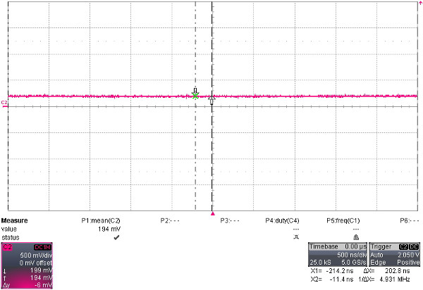
The COMP pin has a level below 0.6V as expected and oscillates around 195mV (30mV pk-pk).
The TPS65400 is running at 1.1MHz with a clock divider of 2 for an actual frequency of the switchers of 550kHz, the COMP pin has a type 3 compensation network whose values are (for the 5V rail) : Croll = 15pF , Rc = 30kohm , Cc = 4.7nF and on the feedback pin there is also a Cff = 1nF.
The same problem is also present on other, more sensitive, rails like the 1.0V and 1.2V that provide power to the FPGA transceiver section, and the voltage output of these rails raises above the recommended operating conditions of the transceivers when the FPGA is not programmed to use the MGTs.
The configuration of the TPS65400 for channel 3 (page 02, the 5V output channel) is as follows:
<register code="10">0000</register>
<register code="D0">0000</register>
<register code="D1">0000</register>
<register code="D2">0014</register>
<register code="D4">0001</register>
<register code="DC">0007</register>
<registerWithPage code="D3" page="02">0000</registerWithPage>
<registerWithPage code="D5" page="02">0005</registerWithPage>
<registerWithPage code="D6" page="02">0000</registerWithPage>
<registerWithPage code="D7" page="02">0005</registerWithPage>
<registerWithPage code="D8" page="02">0014</registerWithPage>
<registerWithPage code="D9" page="02">0003</registerWithPage>
<registerWithPage code="DD" page="02">0004</registerWithPage>
<registerWithPage code="DE" page="02">0000</registerWithPage>
<registerWithPage code="DF" page="02">0000</registerWithPage>
<registerWithPage code="F0" page="02">0010</registerWithPage>
<registerWithPage code="F1" page="02">0001</registerWithPage>
<SchematicLabel id="CSS3">0.1uF</SchematicLabel>
<SchematicLabel id="RFB1SW3">13.089kΩ</SchematicLabel>
<SchematicLabel id="RFB2SW3">2.499kΩ</SchematicLabel>
I have followed the design guidelines as stated on page 65 of the datasheet, the Power traces are on the top layer and inner planes and the noise sensitive Vfb and Comp networks are on the bottom layer for a compact layout with traces as short as possible.
Has anyone experienced similar issues? Is there a maximum off-time of the switcher when in burst mode?
Thanks in advance for the replies
