This thread has been locked.

If you have a related question, please click the "Ask a related question" button in the top right corner. The newly created question will be automatically linked to this question.

about tl494 feedback

Other Parts Discussed in Thread: TL494

I ask you: often see the connection TL494 feedback received error amplifier inverting input, and connected to the inverting input of the reference, TI gives the official application is the same. Can it use the feedback received error amplifier inverting input, and then with reference to the input and PWM output transistors from the collector C to a pullup resistor connected to VCC output? Why do I use the BUCK circuit, there will be no output? Other feedback PWM control chip is connected to the inverting input terminal, and why 494 is an exception
  • User,

    The error amplifiers and output transistors are fully accessible via the device pins. Almost any configuration is possible.
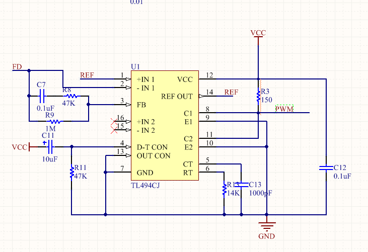
    Can you supply a schematic or block diagram of the buck configuration you are using?
  • Schematic has been uploaded. I guess the reason is this: because of the dead zone control, when the feedback received at pin 1 , the initial state is a feedback is 0V, the error amplifier output to 0, and then superimposed on the dead and the sawtooth comparator generates 94% duty cycle the PWM. But instead, the feedback received at pin 2 , the initial state of the error amplifier output high and compare 0% duty cycle , reverse through the transistor collector, output a 100% duty cycle. For the high-side bootstrap driver MOS, 100% duty cycle is unable to bootstrap capacitor charging and discharging, so MOS can not be opened. if i guess right ?
  • User,

    The first thing to try is connecting pin 16 to ground and pin 5 to pin 14. This will disable amplifier 2. With the inputs floating, the effect of amp 2 is unknown.