This thread has been locked.

If you have a related question, please click the "Ask a related question" button in the top right corner. The newly created question will be automatically linked to this question.

Opposite external "pull" consideration in bq78350

Other Parts Discussed in Thread: TIDA-00255

Hi,

In bq769x0 and tida-00255 “pulling” is frequently assumed for where it is improbable. For example as in fig.7-3:

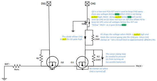
Q1: (PACK-) has been assumed both low and high. For proper design PACK- should the lower side of the pack and cannot be high.

The zener in parallel to 1M R2, is it for the erroneous case the PACK- is connected to HIGH of the external charger, and PACK+ to low, so opposite voltage is applied. Only in this case I saw how 1) the zener clamps voltage 2) as the side note to 1M R1 describes R1 as limit the current when PACK- pulled high.

So are they just fault-tolerant countermeasures?


Q2: (PACK-) could also be a trifle higher than VSS when discharging, but this is only due to RDSon of Q1 and Q2.

1)     This should have been already considered by the designers, is it?

2)     In this case even PACK- is higher than VSS, due to FET’s symmetry, Q3’s drain would be slightly higher than gate, and it is hard to say whether this marginal voltage due to (RDSon,Q1 + RDSon,Q2) can even exceed VGSth of Q3.

So I feel this case is ignorable, and the circuit as mentioned in Q1 essentially is to prevent externally applied opposite voltage.


Calino

  • During normal operation with both FETs on and either a charger or load present, PACK- will be near BATTERY- (and VSS) depending on the load as you indicate.

    Normally the charger should not overcharge the battery, a load should not over-discharge the battery and the temperature should stay in a safe range.  However if any of the protections need to prevent charge or discharge, then PACK- can move from BATTERY- (and VSS).

    If the discharge FET is off with a load, PACK- will be pulled to PACK+.  The circuit is designed to prevent damage to the IC in this case.

    If the charge FET is off with a charger present and the charger voltage is greater than the battery voltage the circuit is designed to prevent damage to the IC and allow the charge FET to remain off.

    Q1 charge FET and Q2 discharge FET should be selected to provide low voltage drop across the FETs when on, appropriate for the application.

    Q3 will be on when CHG pin is high whether from internal register command or from pull up by PACK- being pulled up by a load when the Q2 discharge FET is off.  The body diode of Q3 will raise the source voltage in this case and the FET will turn on with sufficient Vgs.

    If Q2 has sufficient voltage rating and R1 is large enough to limit the current to a safe value, the circuit can survive reverse voltage application.

  • "Since CHG clamps at ~18 V, R1 will limit to approximately V(PACK–) /R1", as in annotation at Figure-7-3, perhaps this line also misses (-18V,) and should be ((VPACK-)-18)/R1?