


Hii all,
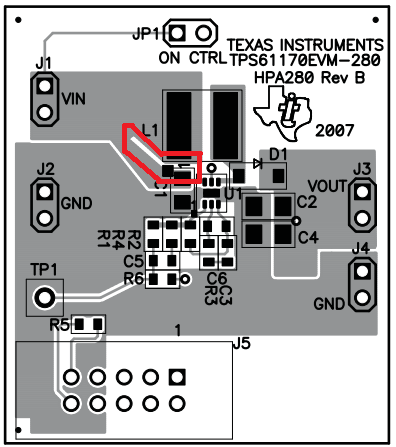
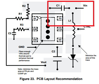
I have been doing a 5V to +4V...+17V variable controlled output design using the TPS61170. For the layout guidelines I referred to the datasheet and also looked into the sample layout of the TPS61170EVM. While looking on the TPS61170EVM boad layout the supply island has been divided by a wedge between the input capacitor terminal and the input to the inductor while no such thing has been explained in the datasheet recommended layout.
My question is what effect this separation in the island has on the design. Would be looking forward to your answers.
Best regards

