This thread has been locked.

If you have a related question, please click the "Ask a related question" button in the top right corner. The newly created question will be automatically linked to this question.

TPS61120 typical application Figure 16 - IC knock out after some use

Other Parts Discussed in Thread: TPS61120

I am deeply in trouble with TPS61120. It has unique power save features and low power dissipation but I cannot work it out properly.

I have set the output of swmode section to 5.5V and set the LDO section to 5V. Used the design which has given on datasheet Figure 16. After successfully working with the IC at the beginning, after some use, it drops the output voltage to Vin+400mV. Basically it breaks down and never revert back. Switch mode feed back voltage drops to 300mV as well which has to be 500mV according to the datasheet. I think I do damage the IC somehow. What cautions do you advice to protect the IC ? I am careful about ESD and hot plug situations.

  • Hi Emre,

    Thank you for the detailed explanation. To properly address your query, I will move this to the appropriate forum so specialized attention can be delivered.

    The Simple Switcher forum focuses on Ease of use solutions for the broad market. Let us know how we can help!

    Thanks,
    Anston
  • Hi Emre,

    It's strange that IC works well but failed after sometime, we have to find what happened after "sometime" and then get the root cause. Please also share some detailed information about the following items:

    1) What's the load condition? Is there some serious load transient at the output of Boost or LDO?

    2) What's input voltage source? A battery or constant voltage source? If it is a battery, does it have large inner resistor?

    3) Is it possible to get the some waveform of Vout, Vin, Iload... just when Vout drops? It can help a lot to find the root cause.

    BR

    Gene

  • Gene Lu said:

    Hi Emre,

    It's strange that IC works well but failed after sometime, we have to find what happened after "sometime" and then get the root cause. Please also share some detailed information about the following items:

    1) What's the load condition? Is there some serious load transient at the output of Boost or LDO?

    2) What's input voltage source? A battery or constant voltage source? If it is a battery, does it have large inner resistor?

    3) Is it possible to get the some waveform of Vout, Vin, Iload... just when Vout drops? It can help a lot to find the root cause.

    BR

    Gene

    Thank you for your attention Gene Lu, I have caused some misunderstanding because of my bad English. Sorry for that.

    By saying "After successfully working with the IC for sometime, it drops the output voltage to Vin+400mV "  I mean, it never comes back again. Like it is getting broken after some use. Then, I unsolder the IC and replace it with a new one. It happened 3 times. After changing it, it works well again but somehow, it malfunctions like I say after some use. It is bizarre because TPS61120 can handle short circuit situations and has a temperature safety control.

    2) What's input voltage source? A battery or constant voltage source? If it is a battery, does it have large inner resistor? :

    Primary input voltage source for this circuit is  3.3V DC bypassed with 470uF electrolytic and 1uF ceramic caps, draws fairly flat voltage line on oscilloscope. Current limited to 700mA but circuit never reaches to that current limit while in use.

    TPS61120 is connected to an Atmega328 via its control pins PGOOD and LBO. TPS61120 Enable pin is driven by a PCH mosfet which connects VBAT pin voltage to EN pin with uC command. Atmega328 voltage source is also 3.3VDC.

    LDO EN pin is driven directly by Switchmode output voltage like in datasheet figure 16. So voltage LDO IN < LDO OUT situation never happens. It powers up an opamp and a pressure sensor totally not more than 100 mA. Also it continues to work after failure situation but cannot reach to 5V as input voltage drops to 3.7V.

    SKIPEN Pin is also directly connected to VBAT pin. ( can be seen on 1st screenshot.)

    1) What's the load condition? :

    Here I attach the critical load for the circuit which is powered by SWMODE 5.5V. It is a motor which draws 300mA at 5.5V when driven directly from DC. In this circuit, it is PWM controlled by uC.

    LDO IN is also sourced from 5.5V SWMODE output. There is no other connection to this 5.5V SW mode power line.

    LDO OUT is source for a pressure sensor and a quad opamp which draws fairly low current like no more than 100mA.

    3) Is it possible to get the some waveform of Vout, Vin, Iload... just when Vout drops? It can help a lot to find the root cause.

    Sorry, it happens suddenly but not after a very distinctive situation. And never comes back again as I mentioned. It totally fails.  But here are some acts that I do with circuit, which might cause the fatal failure.

    1- I do connect and disconnect a programming cable to Atmega328 RX TX RST and GND pins. GND is common but uC powers up from direct voltage source which is 3.3V

    2-  I do drive the motor with 5.5V VOUT - it has flyback diode and back EMF cap 10uF and 47nF

    I am not sure what happens,  maybe ESD, also I am trying to not make hot plug, always connect board first and main power supply second which has soft start...

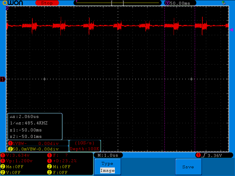
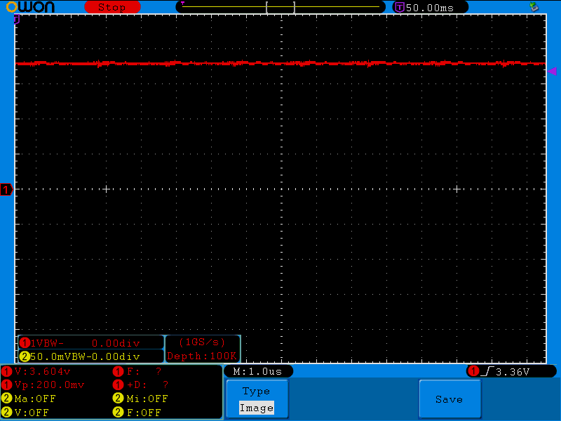
    Here are some additional oscilloscope screenshots...

    LBO Low Battery Out Pin : HIGH 3.2V

    PGOOD Power Good Pin : LOW - 50mV

    Input Voltage 3.2V - connected to 10uH L1 and VBAT pin

    VOUT voltage 3.63V which is supposed to be 5.5V but always results as VIN + 400mV - also at the beginning, it was a clear 5.5V

    FB Pin which is supposed to be 500mV - see the R3 and R4 at the first post first screenshot

    LDO Out voltage, which seems well as input is 3.63V for LDO IN

    Thank you for your time. This is a prototype and we want to use this IC in a battery operated hand held system if we would succeed.

  • Hi Emre,

    Sorry for my late reply.

    The detailed information is really helpful.

    1) Let's firstly confirm whether it is broken by thermal problem or not. The IC has the thermal protection, so if it is really broken by the thermal problem, IC should be very hot. Would you please touch the IC to feel whether it is very hot just when it just fails to work?

    2) From the output voltage waveform, the "Switching frequency" is just around 500kHz, it seems that IC try to work normally.

    3) From the input/output information, Vin is 3.2V with 700mA current limit, and Vout is 5.5V with 400mA output current. The load is really heavy and may touch the "700mA" limit. I guess the "sometime" when IC fails to work is just the time when Motor drive load and sense load are both fully on. Please enlarge the current limit of input voltage source or reduce the load to see if the IC can work normally.

    BR

    Gene

  • 1) It does not warm up after got broken but I it was hot before broken up. But the problem is, I do not know why it does get hot and fails.

    3) Enlarging the current limit did not work. My current limiting voltage source lights up a red led if it goes to CC mode and I have not  seen that light ever lighting up during the operation. No problem with limiting I guess..

    For update, I did change the TPS61120 again, it works well again for 2 days. I did some extra modification on the circuit for being cautious. I did put a 100uF tantalum cap parallel to the input source - between VBAT and CHGND at the design - , so I guess, when I disconnect the board from the input source, it drains out the input voltage slowly and in this way, output of the IC would be more stable while bleeding out the last drop of the voltage.

    Also I have added 2 Schottky diodes parallel to the voltage lines. One is at the input of the IC between VBAT and CHGND, other is at the output of the IC between 5.5VDC and CHGND. I hope it may prevent any spike through the IC like a flyback diode.

    • So, when you look at the design that I've shared, is there a design mistake that causes to fail the IC. I have shared the motor driver design, which is the only part driven with the booster side of the IC, may it cause the failure ? The PWM driver design is obvious and I cannot see a mistake about it.
    • Do you think 10uH L1 placed OK in the PCB design, may it cause any failure ?
    • May misuse of EN pin cause any problem because of any software issue ?
    • Does placement of the 0R resistor R63 may cause any problem which connects CHGND and GND of the IC

    Thank you for your consideration.

  • About your question:

    1) The schematic of boost and motor drive is OK.

    2) It's suggested that L1 placed as close as to the IC, especially the trace between SW pin and L1. Otherwise the ring voltage at SW pin will be high. If possible, FB pin resistors should also be placed close to IC.

    3) EN pin is OK since it's controlled by external signal.

    4) It's OK to add the R63 between two GND.

    If it works well with large input cap, would you please share the SW voltage and Vin voltage? And compared with the test condition without large input cap?