This thread has been locked.

If you have a related question, please click the "Ask a related question" button in the top right corner. The newly created question will be automatically linked to this question.

MOSFET "CSD19536KCS" SOA - Query

Other Parts Discussed in Thread: CSD19536KCS

Hello,

I am using MOSFET “CSD19536KCS” for my Motor drive Project.

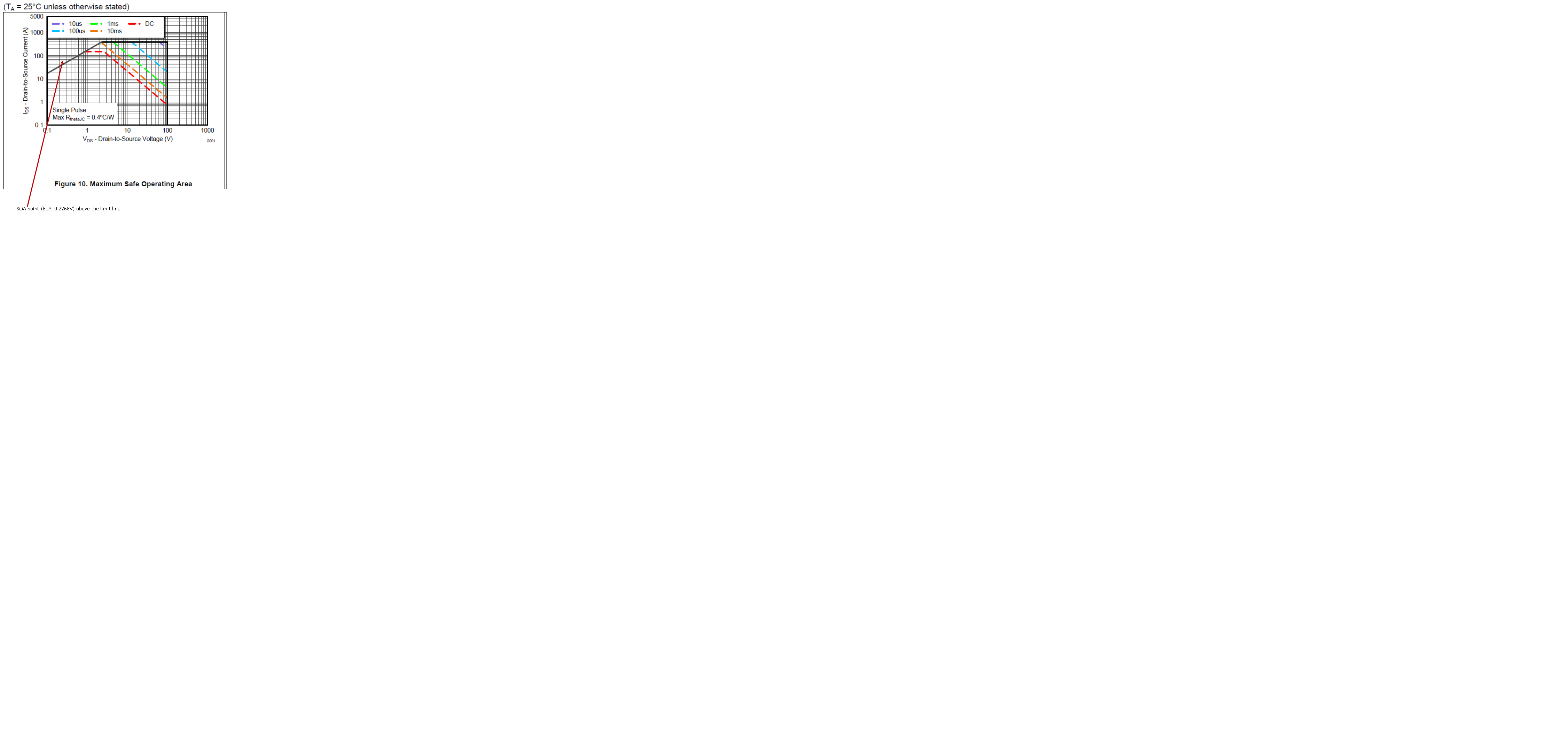
Currently I am trying to find out SOA of MOSFET for my application.

Specs & Calculations:

Drain Current Ids: 60A

Max Tj = 85 Degree C (To be maintained)

Rds. ON max = 1.4*2.7 m Ohms = 3.78 m Ohms (from datasheet normalized Rds. ON curve figure.8)

So, Vds = 60*3.78 m= 0.2268V

If I mark these Ids (60A) and Vds (0.2268) values in SOA graph, SOA point is going above the Rds ON limit line. (see attached image)

I understood that, datasheet Rds ON limit line is drawn for Rds ON@Tj=175 Degree C. (Which is nearly 2.15*2.7m Ohms=5.80 m Ohms).


But how do I explain my self whether my MOSFET is in SOA or not , as SOA point is above the limit line?? Kindly explain.

Regads,

Govind.


  • Hello ,
    I have missed to mention one important Input parameter. That is Vgs.
    gate to source Voltage Vgs= 10V. (I want operate MOSFET in saturation/fully ON mode )

    Kindly clarify. Your inputs would help me a lot to proceed further.

    Regards,
    Govind.
  • Govind,

    The SOA is a check to make sure you are operating within its confines when the MOSFET is operating in the linear region. The Rdson line limitation is taken from what the current will be limitted to when the Rdson is at its max possible value, at the maximum allowable temperature of the FET.

    So even though you are outside the SOA, if you keep the junction temperature to 85deg, you should be fine. Eventually, the amount of current you can push through the FET when fully enhanced will saturate, but for the CSD19536KCS, this will be much greater than 60A.

    All that to say, if you ensure that Tj = 85, you should have no problem operating at 60A.

    A better figure to refer to for your question would be figure 10. By maintaining the case at 85deg (I'm not actually sure how you could gaurantee you were maintaining the junction at 85), you should be well within the current limits of the device.

  • Hello Mr. Brett Barr,

    Thanks for the explanation.
    To give you more explanation on maintaining the Tj@85, i would like to mention the details of my design.

    My actual current requirement is 180 A rms. I am using total 6 MOSFETS in parallel (30A for each). With this power dissipation(3.4W per MOSFET), we did thermal simulation and designed heat sink. We are able to maintain the Tj@85.

    Current requirement is to reduce the number of mosfets and analyze how many MOSFETS can be reduced still maintaing the Tj@85. This is trade of between MOSFETs reduced cost and heatsink increased cost.
    However Increase in Tj to 95 (de-rating limit) shall be considered depending on the cost saving.

    Kindly, Let me know if any thing needs to be discussed/mentioned here and i missed it.

    Regards,
    Govind.
  • Hello Mr. Brett Barr,

    I have one more query.

    Is there any way to simulate Junction temperature value for different case to ambient Thermal resistance and for different ambient temperatures in TINA software??

    Kinly suggest.

    Regards,
    Govind.
  • Govind, I am not too familiar with TINA software but I can inquire about this.
    However, once you know the specific thermal resistance of your design, calculating the junction temperature is a relatively straight forward calculation. Is there a reason you want to do this in TINA?
  • Hello Mr. Brett Barr,

    I would say yes. We are planning to perform the CFD simulation. As it is little costly, we want check simulation results first to get an initial understanding on heat sink design. This gives us a confidence on compatibility of heat sink as per our enclosure design.

    If i can get the thermal simulation model of MOSFET (RC network model, or similar), it helps me a lot.

    Regards,
    Govind.
  • Govind, I have asked the engineer who writes our spice models. I will let you know his response.
  • Hello Mr.Brett Barr,

    I am pleased to wait until the response comes from concerned team. Meanwhile, i need an expert opinion on below topic.

    As per my de-rating guidelines , maximum allowed solder joint temperature(continuous) MOSFET is 95˚C. what could be the difference temperature between MOSFET junction and MOSFET Drain lead pin (not exposed pad)? i am expecting nearly 2˚C. is it a good approximation??

    Regards,

    Govind.

  • Govind,

    Lead temperature is very dependent on the heat sink and the board conditions. However, you are correct in that the drain pin is the best thermal indication of what the junction temperature will be. Talking to some experts, they would anticipate that this should fall within 2-3deg of each other.

    As an asside, have you been working this issue with any TI FAE or sales? I only ask because we have recently had a very similar question come in from internal TIers.

  • Hello Mr.Brett Barr,

    Sorry for the delay in response.
    Yes, we have already contacted TI sales team in Bangalore, India. Meanwhile, i have posted this query to get an approximate value which helps us to proceed with our CFD simulation.
    Kindly let us know if any progress on this topic.

    Regards,
    Govind.
  • Govind,

    See the attached thermal model:

    CSD19536KCS_thermal.TSC