This thread has been locked.

If you have a related question, please click the "Ask a related question" button in the top right corner. The newly created question will be automatically linked to this question.

TPS43061 - About EN to start switching time

Guru 21045 points
Other Parts Discussed in Thread: TPS43060, TPS43061

Hi Team,

We would like to know about EN to start switching time(tEN).


-----------------------------------------------

[Q1]

I understand that “tEN” is the following figure.

Is my understanding correct?


-----------------------------------------------


[Q2]

Does “tEN” depend on "Cvcc"?


If yes, could you please let us know the method of calculation of this time?

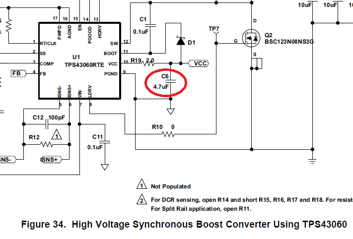
So, our customer would like to know about following contents.


-If "Cvcc" is bigger than 0.47uF, does "tEN" increase?

-If "Cvcc" is smaller than 0.47uF, does "tEN" decrease?

-Could you please let us know the max and min value of “tEN” at “Cvcc=4.7uF”.

Because, they referred to "Figure34" to design the circuit.

I would be grateful if you could reply as soon as possible.

Regards,

Kanemaru

  • Hi Kanemaru-san,

    The CVCC capacitor only has a small impact on the delay in this waveform. The influence is how long it takes for the CVCC capacitor to charge up to regulation. This looks to be about 250 µs in these screenshots. The main reason for the long delay in switching on the EVM is because VIN will pre-bias VOUT through the body diode of the high-side MOSFET. SS needs to reach FB before the TPS43060/TPS43061 can start switching.

    I don't have data readily available on the influence of the capacitor on the delay to start switching. A min and max most likely does not exist so it would take some time to look into this. However I suspect they may not need this anymore after understanding the reason for the ~13 ms delay is the pre-bias to the output from VIN.

    Best Regards,
    Anthony

  • Hi Anthony-san,


    Thank you for the information!

    So, I understand that “this delay time” depend on “Css” and “VFB at startup timing”.

    Therefore, I understand that the calculation methods of "delay time" are as follows.

    Is my understanding correct?


    ---------------------------------------------

    <calculation of VFB at startup timing (refer to Equation4)>

    Vout(pre-bias)/((RHS/RLS)+1)= around 0.6516V


    [Parameter]

    -RHS=124.0449kohm (refer to page21)

    -RLS=11Kohm (refer to page21)

    -Vout(pre-bias)= around 8.0V (refer to Figure24)

    ----------


    <Calculation of delay time (refer to Equation9)>

    (Css*VFB at startup timing)/Iss= around 13ms


    [Parameter]

    -Css=0.1uF (refer to page21)

    -Iss=5uA(refer to page7)

    ---------------------------------------------


    Could you please let us know if you have any concern?


    Regards,

    Kanemaru

  • Hi Kanemaru-san,

    Your calculations for the delay due to the pre-bias looks good.

    Best Regards,
    Anthony
  • Hi Anthony-san,


    Thank you for your reply.

    I greatly appreciate your cooperation!


    Regards,

    Kanemaru