LM3478 based SEPIC Supply Misbehaves after 3rd PCB spin
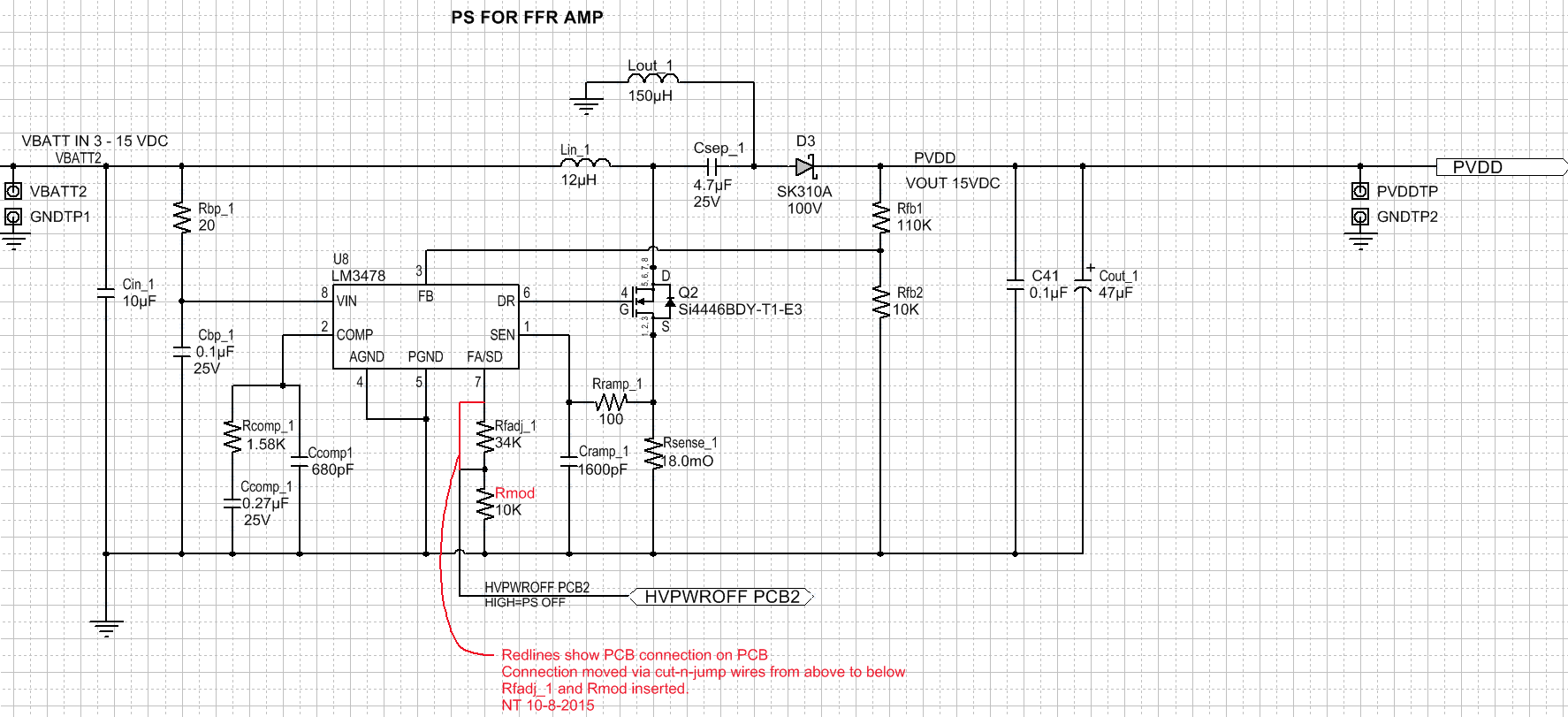
Two years ago with Web Bench I designed a SEPIC supply using LM3478 to output 15 VDC @ 0.5A from an input of 3 to 15 VDC. The power supply feeds a 30 watt class-D audio amp IC including 450 uF decoupling capacitance on the chip’s power input pins. The schematics are shown below. Now on our third PCB layout the power supply + audio amp design has worked very well in lab and field testing.
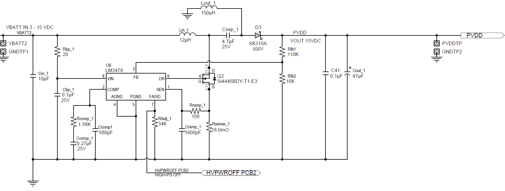
SEPIC supply using LM3478 9 VDC in to 15 VDC Out
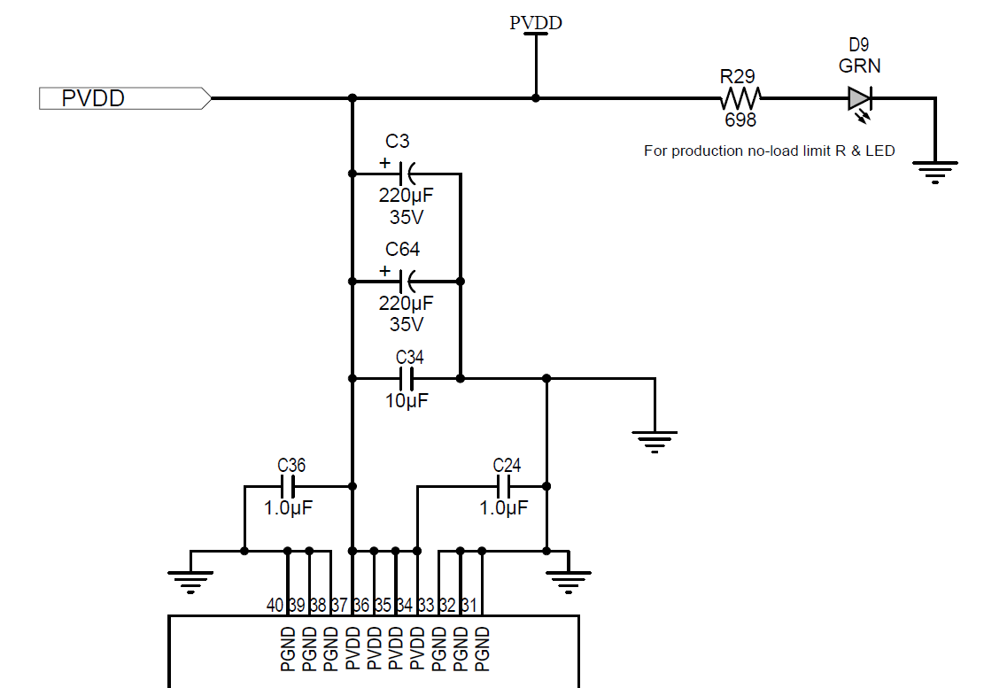
Supply load is 30 watt class-D audio amp with 450 uF decoupling capacitance
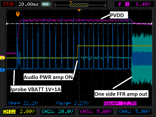
While checking the third revision of the PCB an anomaly was noted. Very large current inrushes on the input and larger than normal supply currents used during operation.

NOSCAP edited.bmp
The top trace of the scope capture shows PVDD the 15 VDC output of the supply come on under MPU control one division in. The middle trace is a clamp on current probe monitoring the circuit’s DC input current, when PVDD switches on 19 A(!) spikes are seen for one major time division. After 100 mS the DC input current drops to ~12 A, note this occurs when signal appears on the bottom trace labeled V@FFR. V@FFR is the amplifier’s output across the load, seriously under sampled at this scope setting it is actually a full scale 10k sine wave. Therefore we see this misbehaving power supply circuit pulling 19 A peaks while being asked to supply 15 V @ ~12mA to an idle power amp then dropping to 12 A peaks 5 A averages when the power amp begins delivering power to its load.
amp_on_0edited.bmp
In the scope capture above time base is 5x faster to look at the time prior to load being applied. I also had my teammate who writes the firmware for this device separate the turn-ons of the power supply and power amp to check the effect of the amp on the supply. Scope triggers from PVDD turning on with its load off. After 100 mS the MPU turns on the power amp as shown on the CH1 yellow trace, based on the frequency of the ~20A spikes on the DC input current probe the power supply circuit takes no notice of the amp turning on. After another 100 mS the MPU begins outputting the 10k sine wave. The power supply circuit does notice the signal turning on and we see the expected frequency increase of the current being drawn from DC input and a welcomed reduction in amperage.
After other circuit checking and debugging efforts I looked at the circuit asking ‘where is all that current going’. The path from Q2 source to ground via the sense resistor looked likely. I tomb stoned the 18 mOhm Rsense_1 and added a wire loop to allow the current probe to be clipped on.

Isense_0 edited.bmp
The scope capture appears to show the excessive current being drawn from DC in is ‘shooting thru’ (to borrow a phrase from H-bridge circuits) Q2 and Rsense_1 to ground.
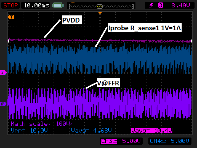
IsenseZnm edited.bmp
Zoomed capture of current at Q2 and Rsense_1 to ground node while circuit under load delivering signal to amplifier’s output load. Current through Q2 and Rsense_1 is peaking at 10 A averaging 4.68 A.
At this time I welcome all suggestions as to why this circuit has gone bad in its adolescence. Is my theory the excessive current being drawn is ‘shooting thru’ Q2 and Rsense_1 to ground plausible? Or is it just charge flowing back into the input inductor via ground? What has made this good circuit go bad?
LM3478 3 to 15VDC in 15VDC out PS no2 Webench Design and Reports.pdf