This thread has been locked.

If you have a related question, please click the "Ask a related question" button in the top right corner. The newly created question will be automatically linked to this question.

LM3445 Current Limit Operation

Other Parts Discussed in Thread: LM3445

On page 23 of the LM3445 data sheet and design guide (document SNVS570L) this paragraph appears:

"Current Limit:

Under normal circumstances, the trip voltage on the PWM comparator would be less than or

equal to 750 mV, depending on the amount of dimming. However, if there is a short circuit or an excessive load

on the output, higher than normal switch currents will cause a voltage above 1.27V on the ISNS pin which will
trip the I-LIM comparator. The I-LIM comparator will reset the RS latch, turning off Q2. It will also inhibit the Start
Pulse Generator and the COFF comparator by holding the COFF pin low. A delay circuit will prevent the start of
another cycle for 180 μs."

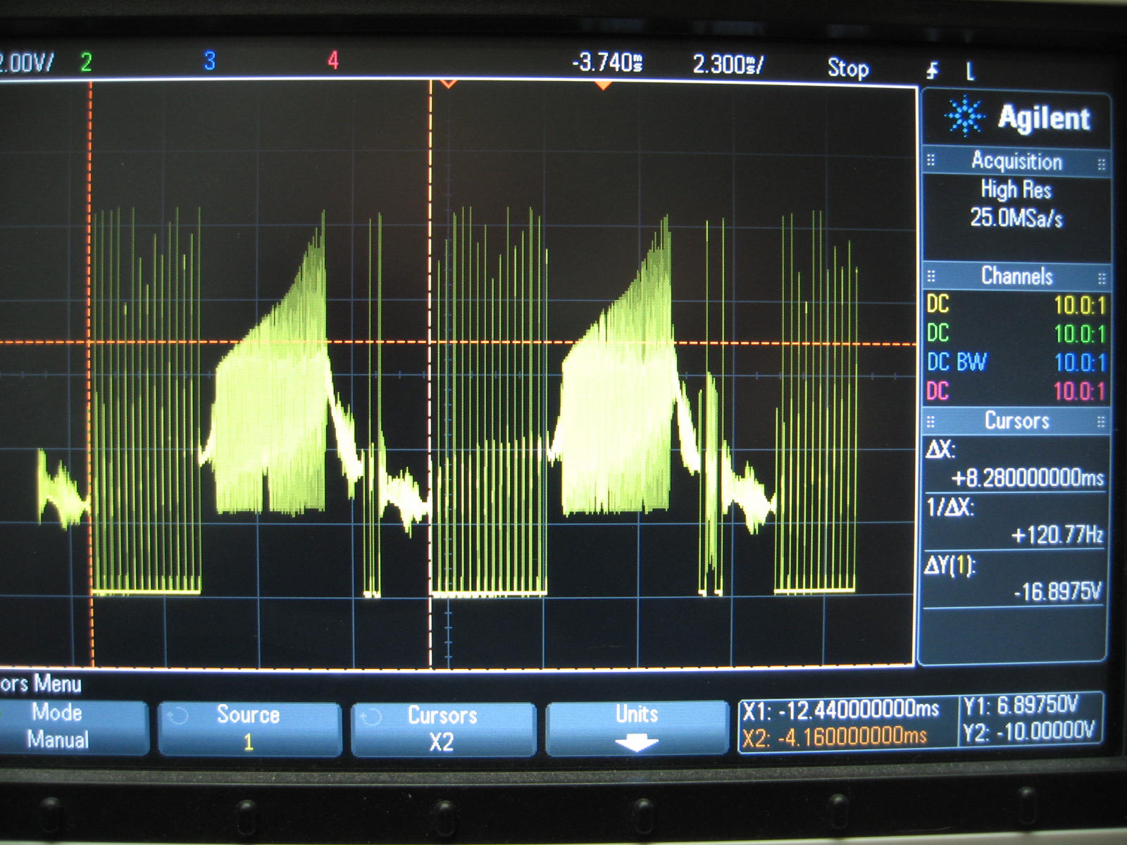
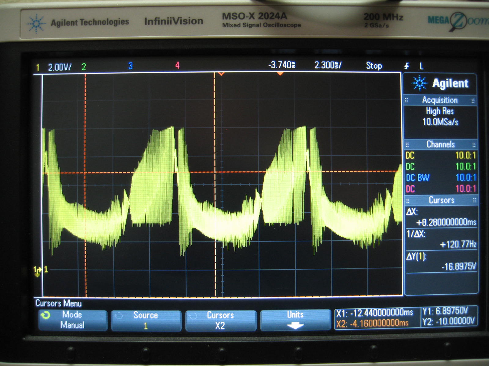
I do not understand the interaction of the PWM comparator and the I-LIM comparator (see Figure 11 on page 7).

It would seem that once the voltage at the ISNS pin exceeds 750mV, the PWM comparator will be tripped and the gate drive to the FET will cease.

The paragraph above indicates that, after the ISNS voltage has exceeded the 750mV threshold of the PWM comparator, thereby cutting off the gate drive to the FET,  somehow the current through the FET can continue to increase and eventually produce an ISNS voltage of >= 1.27V to trigger the I-LIM comparator, thereby cutting off the (already cut off) gate drive to the FET.

This seems contradictory.  Can someone please explain?

  • Ideally under normal operation the PWM comparator is under control, the ILIM comparator is only for current limit protection under "fault" conditions. There is always a delay in the PWM comparator so there are circumstances that could cause the current to increase beyond where the PWM comparator terminates and that is where current limit protection comes in. This could happen if the inductor shorts, if there is a fast rising transient at the input voltage, if the output is suddenly shorted, or if the inductor saturates. Any combo would do it as well (inductor near saturation normally then a tranient at Vin that causes it to saturate). The ILIM comparator would then trip and disable the switching briefly to make sure the switch, diode, LEDs, or inductor are not damaged.

  • Clinton,

    Thanks for the reply.

    So, the delay through the ILIM path must be MUCH shorter than through the PWM path in order to prevent switch destruction.

    Here are photos of the voltage waveform at the FET-drain / inductor junction on two LM3445 boards (A and B) that have identical components and are just slightly different in layout. 

    The "Board A " scope trace (shown first below) shows the LM3445 on that board going into what appears to be ILIM protection mode (the pulses are exactly 180 usec apart) during the time that Vbuck is reaching its maximum.  The "Board B" trace (shown second below) has no such interlude.

    I have built two of the "A" boards and both exhibit the apparent ILIM behavior. But since the components are identical on the A anb B boards, I am trying to find the cause of the difference.

    Any ideas ?

    Thanks,

    Benny Smith


  • If you are sure the components are the same, they are populated correctly on both, and that there are no trace routing error on either then the difference is most likely due to layout. Switchers require careful layout and any number of things could cause the part to think it is hitting current limit due to the noise generated. Sometimes it is something small (like running the current sense trace near or beneath the inductor) and sometimes it is something bigger (improper grounding). But if you would like to send me the two layouts to look over I would be happy to comment. Probably more than half the issues I see are due to layout.
  • By the way, schematics would help as well so I know what is where.
  • Please give me your email address so that I can send the schematic and layout confidentially.

    benny@visionsmith.com
  • No problem. E-mail sent.