This thread has been locked.

If you have a related question, please click the "Ask a related question" button in the top right corner. The newly created question will be automatically linked to this question.

bq78350 SMBUS basics

Other Parts Discussed in Thread: BQ78350

Hi All,

Got my custom BMS PCB for a 6S battery pack from the assembly house a couple of days ago. The BMS design is based on the BQ7693000DBT AFE, BQ78350 GG and a host MCU.

After going over the datasheet and the TRM, I was unable to find a single example of an SMBUS transaction for reference, just the small timing plot.

The TRM lists with great detail the register definitions, but lacks a detailed explanation or diagram of a complete SMBUS transaction.

Currently I'm only able to get an ACK after sending the 0x16 slave address, but am clueless regarding the addressing scheme of the bq78350.

Can someone help with an SMBUS example for this device? Even a logic analyzer screenshot of a successful transaction will help.

A short explanation regarding the memory organization will truly help.

What are Class and Subclass - Base addresses?

Your kind help is much appreciated.

SBD

  • I do not have a set of SMBus signals specifically for the bq78350, but the attached document provides waveform examples for the SMBus protocol that we use with all of our SMBus devices. 7455.SMBus made simple_v6.pdf

  • Hi Thomas,

    Thanks for your reply.

    The app note you linked will be really helpful. What I'm missing now is how to read  the data-sheet.

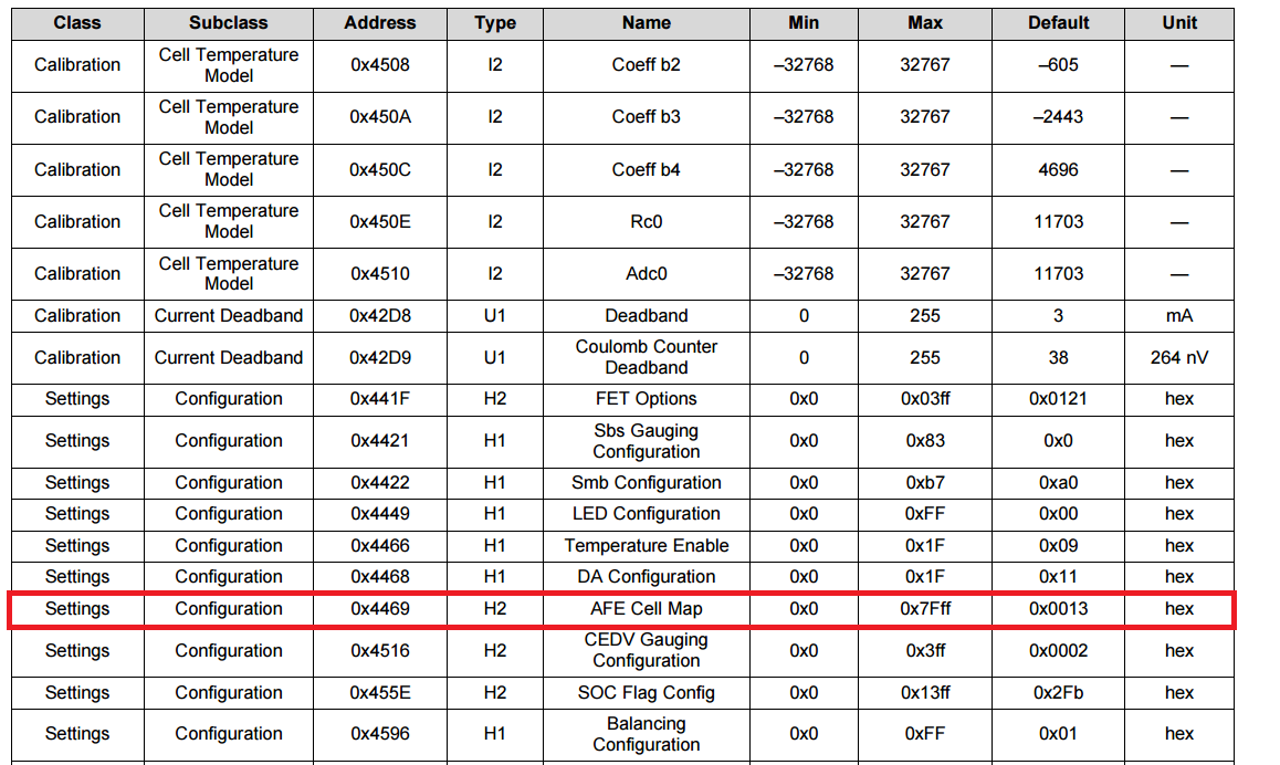
    If I would like to first read the AFE cell Map in order to tell the GG it's connected to a 6 cell pack, how would the SMBUS transaction look like for reading the default configuration from address 0x4469?

    Start Condition

    Write 0x16 - ACK

    0x44 - ACK     (MSB First - ???) 

    0x69 - ACK 

    Re-start condition

    Read 0x16 - ACK    (0x17 read address)

    0x13 - ACK      (LSB First) 

    0x00- NAK

    End Condition

    Am I on the right track here?