This thread has been locked.

If you have a related question, please click the "Ask a related question" button in the top right corner. The newly created question will be automatically linked to this question.

TPS61090 - distance of output capacitor

Other Parts Discussed in Thread: TPS61090, TPS61230

Hello,


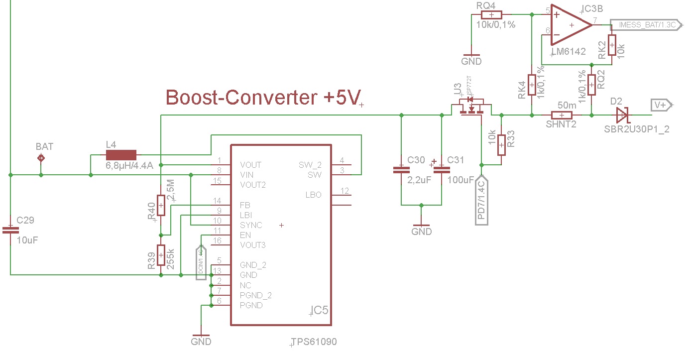
we are using the TPS61090 in one of our products with a LiPo-Battery (3 - 4,2V) input and an adjusted output of 5,3V.
Now we are recognizing that sometimes the device gets damaged after working for hours.
When damaged, sometimes we have a short between SW and GND and sometimes there is no short, but the output voltage stays on ~500mV independent from Vin.

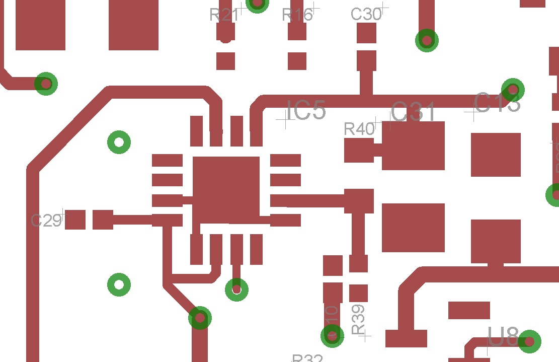
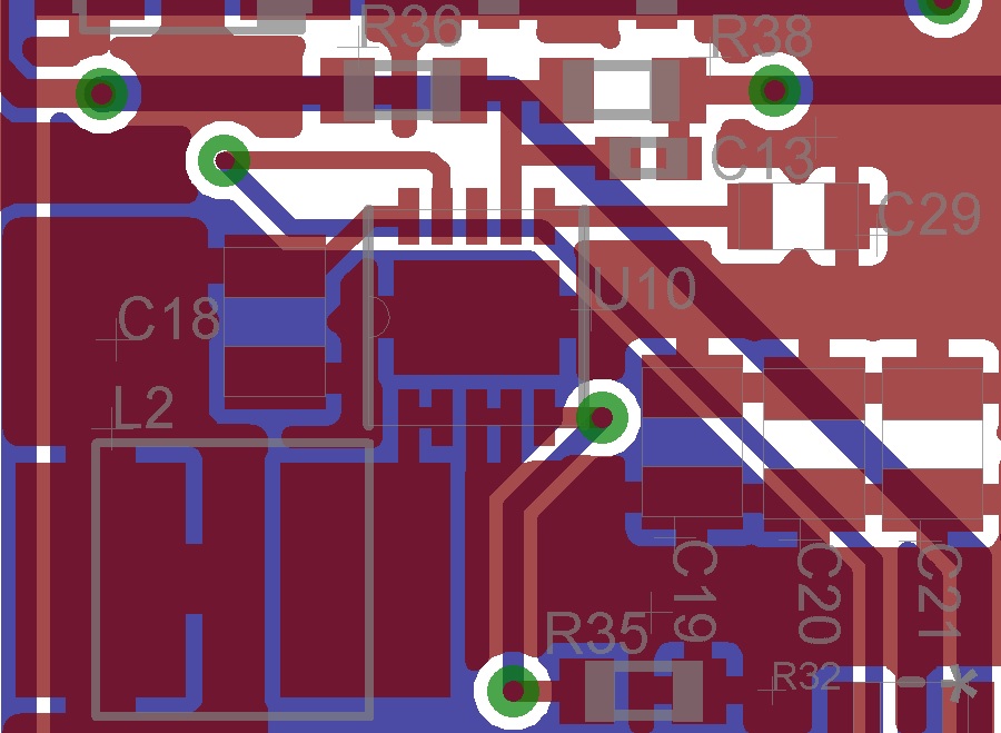
While reading in various other Posts within this forum, a lot of possible solutions was optimizing the layout by placing the output capacitor close to the IC.
So could you please indicate the maximum distance of the output capacitor to the IC in order for the device to work well?

Best Regards,
Patrick

  • hi Patrick

    Sorry for the late reply. it is hard to specify the distance between the Cap and the IC. because the parasitic inductance between the two component not only depend on the distance but also the width, thick and the loop area of the tracks that connects the cap and the IC.

    could you share your layout? i could help to suggest how to improve it.

    and the lipo-battery input application, the TPS61230 will be better solution.

  • Hi Jasper,


    Thank you very much for your response.

    Please find attached our layout as well as the schematic.

    Why do you think, that TPS61230 will be better solution?


    Best Regards,

    Patrick

  • Patrick
    I see some pins is floating. all the VOUT pin and SW pin in the IC should be connected together in your schematic. and please follow the suggestion in the datasheet page 19 for PCB layout.

    TPS61230 is simpler, easy to used and don't need tantalum capacitor.
    what is the output current in your application? there may be other better solution if the output current is small.
  • Hi Jasper,

    thanks for your suggestions.
    So leaving these pins floating could lead to those problems? We found out the the devices will work for a lot of times and then suddenly they get damaged when the TPS61090 is activated by the EN Pin and switch U3 is getting closed to connect the load to the converter.

    The average output current is about 500mA with a maximum of 2A in some cases.

    Best Regards,
    Patrick
  • Patrick
    Yes. the device is designed to connect these pin together to support the high current. the TPS61090 can't support 5V 2A because of the current limit. please change to TPS61230 in this high current application.
    you should follow the datasheet for schematic and layout.
  • Hi Jasper,

    Thank you very much for your support.
    We just modified our schematic and layout by including the TPS61230. Could you please have a look on it an give your statement if this solution will work?

    Thanks in advance.

    Best Regards,
    Patrick

    Vin: 3.0 - 4.2V (LiPo-Battery)
    Vout: 5.3V
    Output current: max. 2A

    U10: TPS61230DRC
    L2: XFL4020-102MEB / Mouser: 994-XFL4020-102MEB
    C18: 22µFarad 6.3V 0805 X5R / Mouser: 81-GRM21R60J226ME39L
    C19, C20, C21: 22µFarad 10V 0805 X5R / Mouser: 963-LMK212BBJ226MG-T
    C13: 16pF 50V 0603 / Mouser: GCM1885C1H160JA16D
    C29: 10nFarad 10V 0603 X7R / Mouser: 81-GRM033R71A103KA1D
    R35: 1MOhm 1% 0603
    R38: 430kOhm 1% 0603
    R36: 100kOhm 1% 0603

    Schematic:


    Layout:

  • schematic : it seem the L2 is not connected to VIN, i can't see the connection dot. others are good
    layout: 1. the track between the VOUT pin and output capacitor is not wide enough.
    2. i would suggest change the polygon connection style, so the GND copper area is as large as possible to help the thermal performance
    3. the layout of the feedback resistors and capacitor is not good, the loop is too long. the C13 should be small package 0402 or 0603 and placed beside R38.
  • Jasper,


    Once again, thank you very much for your support.
    Please find attached the modified layout based on your comments.

    We are now going to produce some prototypes / performing some stress tests and I will come back with the results.

    Best Regards,
    Patrick